

Halftone phase shift mask blank, halftone phase shift mask, and pattern exposure method
a technology mask, which is applied in the field of halftone phase shift mask blank, halftone phase shift mask, and pattern exposure method, can solve the problems of pattern-transfer failure of semiconductor substrates patterned using masks, chemical cleaning can damage the halftone phase shift film on the mask blank or mask, and achieve the effect of facilitating photomask pattern formation
- Summary
- Abstract
- Description
- Claims
- Application Information
AI Technical Summary
Benefits of technology
Problems solved by technology
Method used
Image

Examples
example 1
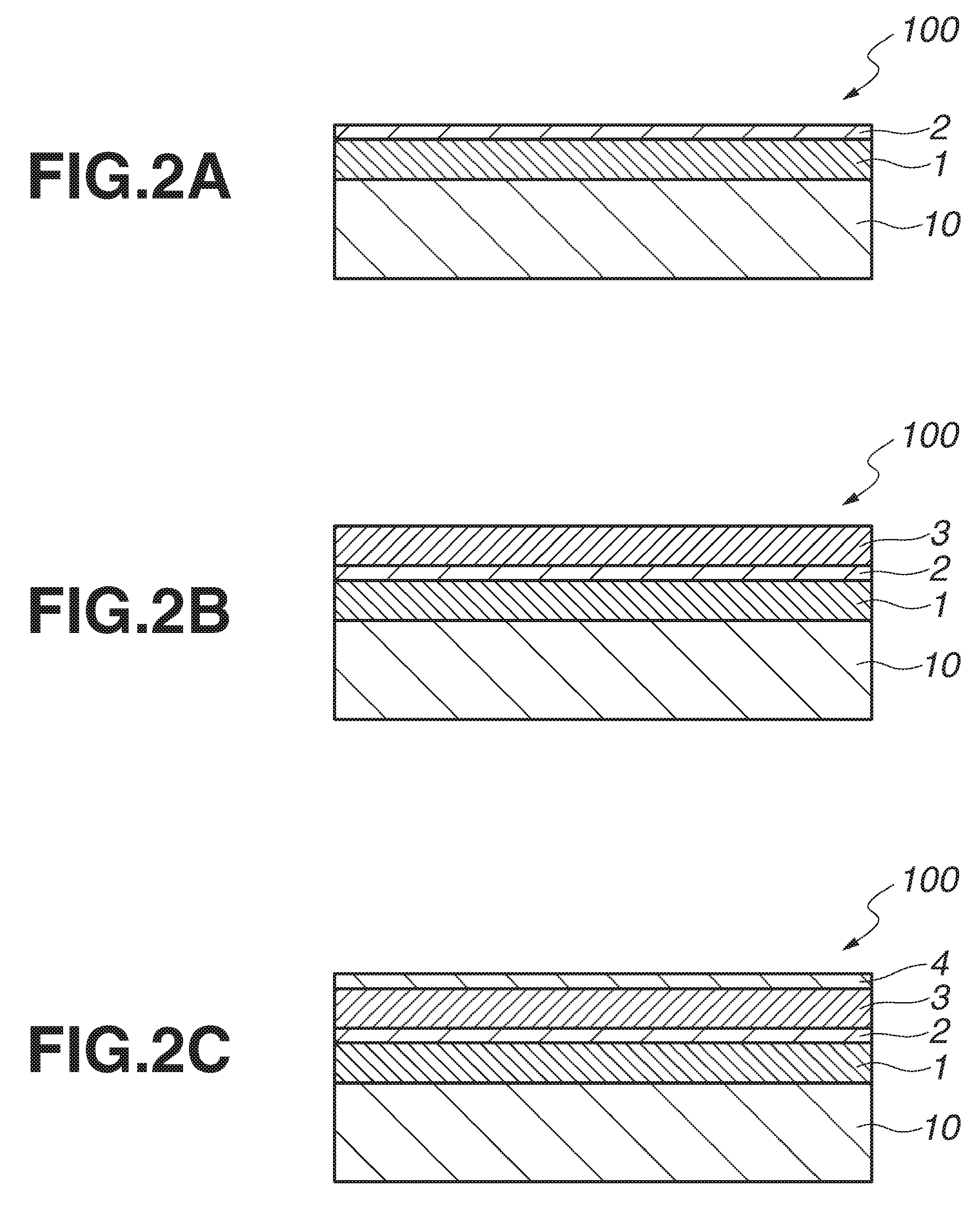
[0090]On a quartz substrate of 152 mm squares and 6.35 mm thick, a halftone phase shift film of SiN was deposited by reactive sputtering using a silicon target as the sputtering target, and nitrogen and argon gases as the sputtering gas. The deposition time was adjusted such that the film might have a phase shift of 178° with respect to light of wavelength 193 nm (ArF excimer laser, same hereinafter). Then the film had a transmittance of 6% with respect to light of wavelength 193 nm and a thickness of 61 nm. On X-ray photoelectron spectroscopy (XPS), the film had a Si:N atomic ratio of 48:52. Also the film had a refractive index n of 2.6 and an extinction coefficient k of 0.64 with respect to light of wavelength 193 nm. The film was examined for chemical resistance by immersing it in an AMP cleaning liquid (28 wt % aqueous ammonia:30 wt % hydrogen peroxide:water=1:1:100 by volume) at room temperature (23° C.) for 120 minutes, after which a change of phase shift was less than 0.10°.
example 2
[0091]On a quartz substrate of 152 mm squares and 6.35 mm thick, a halftone phase shift film of SiN was deposited by reactive sputtering using a silicon target as the sputtering target, and nitrogen and argon gases as the sputtering gas. The deposition time was adjusted such that the film might have a phase shift of 180° with respect to light of wavelength 193 nm. Then the film had a transmittance of 12% with respect to light of wavelength 193 nm and a thickness of 60 nm. On XPS, the film had a Si:N atomic ratio of 47:53. Also the film had a refractive index n of 2.6 and an extinction coefficient k of 0.46 with respect to light of wavelength 193 nm. The film was examined for chemical resistance as in Example 1, with a change of phase shift of 0.40° being detected.
example 3
[0092]On a quartz substrate of 152 mm squares and 6.35 mm thick, a halftone phase shift film of SiON was deposited by reactive sputtering using a silicon target as the sputtering target, and oxygen, nitrogen and argon gases as the sputtering gas. The deposition time was adjusted such that the film might have a phase shift of 177° with respect to light of wavelength 193 nm. Then the film had a transmittance of 7% with respect to light of wavelength 193 nm and a thickness of 62 nm. On XPS, the film had a Si:N:O atomic ratio of 46:50:4. Also the film had a refractive index n of 2.6 and an extinction coefficient k of 0.59 with respect to light of wavelength 193 nm. The film was examined for chemical resistance as in Example 1, with a change of phase shift of 0.24° being detected.
PUM
 Abstract
Description
Claims
Application Information