Package and antenna apparatus including package

a technology of antenna apparatus and package, applied in the field of package, can solve the problems of increasing noise figure, high cost of low-loss pcb substrate, and very limited frequency approach, and achieve the effects of low manufacturing cost, high repeatability, and low loss

Active Publication Date: 2016-10-06
SONY CORP
View PDF7 Cites 60 Cited by
  • Summary
  • Abstract
  • Description
  • Claims
  • Application Information

AI Technical Summary

Benefits of technology

[0010]It is an object of the present disclosure to provide a package for embedding one or more electronic components and to an antenna ...

Problems solved by technology

As the dielectric losses and the losses of the interconnect are very high in E-band, this solution results in an increased noise figure.
Furthermore, expensive low loss PCB substrates are required.
In general, this approach is very limited in frequency.
However, as the antenna is covered by some polymer mold mass and the package features many edges, scattering and diffraction occur.
This has a negative impact on the antenna pattern, which typically results in some ripples.
Using eWLB technology there is little means to improve the antenna performance.
The distance of the backshort depends on the accurate s...

Method used


Image

  • Package and antenna apparatus including package
  • Package and antenna apparatus including package
  • Package and antenna apparatus including package

Examples


first embodiment

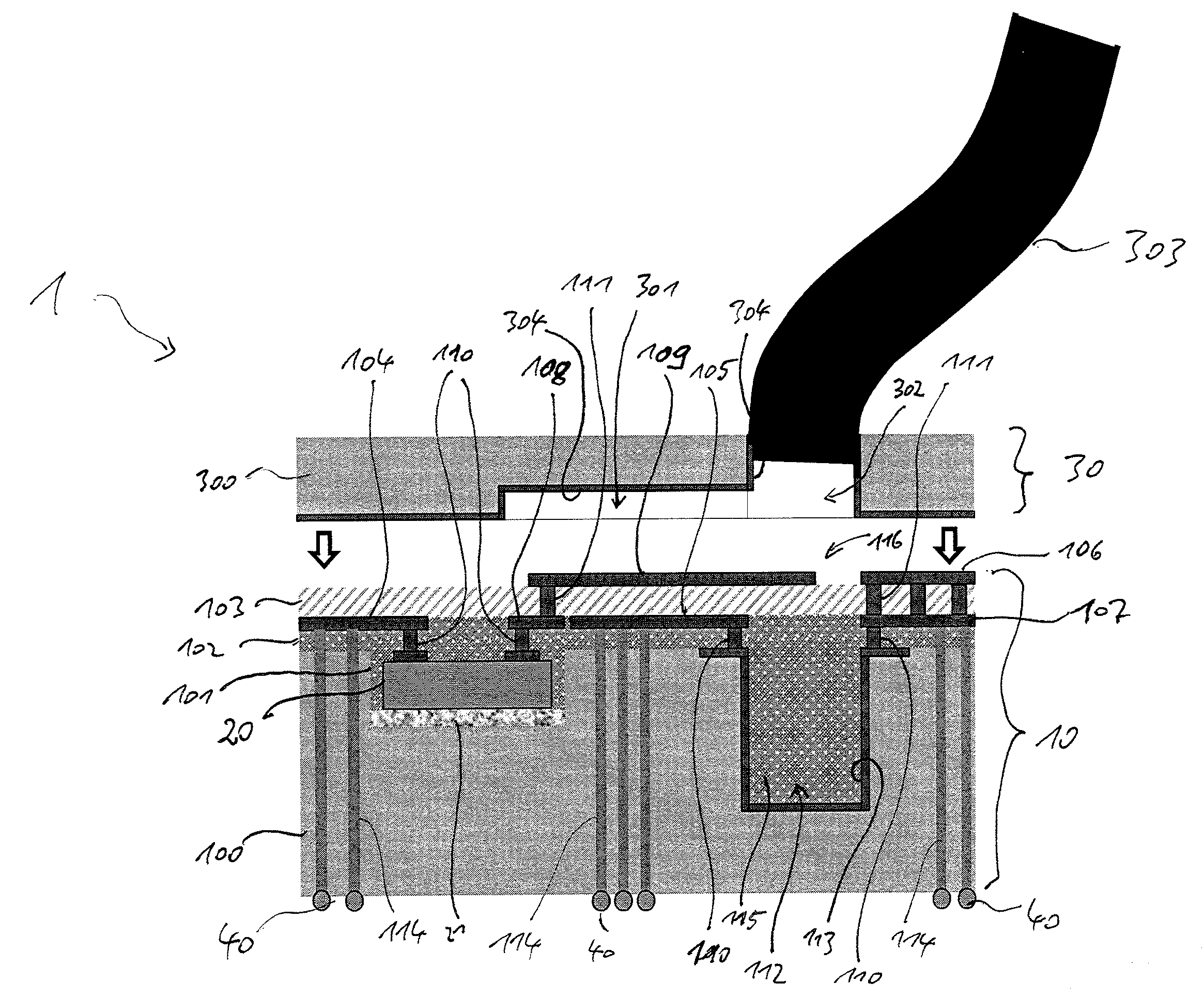
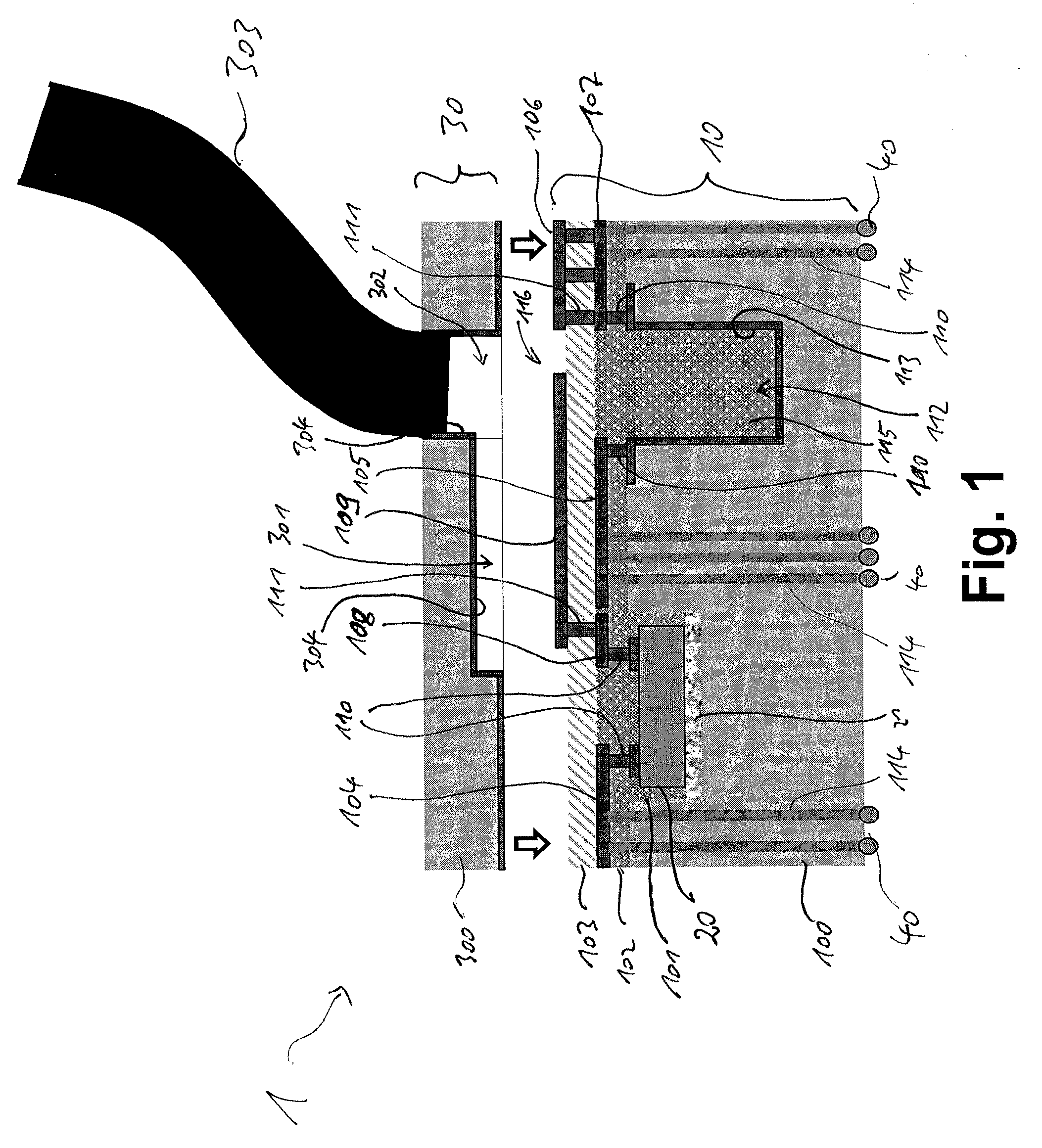
[0056]Referring now to the drawings, wherein like reference numerals designate identical or corresponding parts throughout the several views, FIG. 1 shows a cross section of a package 1 in an intermediate manufacturing stage according to the present disclosure. FIG. 2 shows the same package 1 in a final manufacturing stage. The package 1 comprises a carrier structure 10, one (or more) electronic component(s) 20, e.g. an MMIC, and a cover structure 30.

[0057]The carrier structure 10 comprises a silicon-based carrier layer 100 comprising one (or more) cavity (cavities) 101 for placing (embedding) the one (or more) electronic components 20 therein. The carrier layer 100 may e.g. be a low resistive silicon wafer since it is relatively cheap compared to high resistive silicon wafers. A first polymer layer 102 is formed on top of the carrier layer 100, and a second polymer layer 103 is formed on top of the first polymer layer 102. Metallization layers 104-109 are provided for use as signal...

second embodiment

[0066]Another possibility of antenna integration into the silicon package is depicted in FIG. 5A and FIG. 5B. FIG. 5A shows across section of a package 2 according to the present disclosure and FIG. 5B shows a top of the package 2 having a carrier structure 11 and a cover structure 31. In addition to the rectangular waveguide 305 formed by a trench etched into the cover layer 300, another rectangular waveguide 117 is formed by another trench etched into the silicon-based carrier layer 100 opposite the waveguide 305. These trenches 305, 117 together form a complete rectangular waveguide. In the center of this waveguide a probe feed is realized by a microstrip-to-waveguide transition 116. Alternatively a loop feed 118 can be employed. The probe or the loop, respectively, may be fabricated on a polymer membrane. This membrane consists of the first polymer layer 102 and the second polymer layer 103, which are both applied as thin films. A backshort 119 of a quarter guided wavelength may...

third embodiment

[0068]FIG. 6A shows a cross section of a package 3 according to the present disclosure and FIG. 6B shows a top view of the package 3 having a carrier structure 12 and a cover structure 32. In this embodiment inline feeding of a rectangular waveguide formed by a metallization layer 124 and a trench 306 in the cover layer 300 is used. Therefore, the microstrip line 109 is fed through a hole in the backside wall of a rectangular waveguide. The microstrip line 109 is preferably terminated in a loop 118, which is formed by the microstrip line 109 and a via 125 to the metallization layer 124. An antenna array can either be formed by open-ended. waveguides in the side wall of the package 3 or by horn apertures 123.


PUM


Abstract

A package for embedding one or more electronic components comprises a carrier structure a silicon-based carrier layer, one or more electronic components embedded in one or more cavities formed in the carrier layer, and a cover structure arranged on top of the carrier structure. The cover structure comprises a cover layer and one or more cavities formed in the cover layer. An antenna element and/or a waveguide for connection to an antenna element is formed in and/or on top of the cover layer and coupled to the one or more cavities.

Description

BACKGROUND[0001]1. Field of the Disclosure[0002]The present disclosure relates to a package for embedding one or more electronic components, particularly by use of a silicon-based packaging technology. The present disclosure relates further to an antenna apparatus including a package, especially for use in millimeter-wave frequency systems, and to a method for manufacturing a package.[0003]2. Description of Related Art[0004]State of the art mm-wave radar chipsets at 77 GHz (and above) use so called embedded wafer level ball grid array (eWLB) surface mount technology for soldering on a PCB like an SMT type electronic component. An eWLB package has “hot” interconnects, which means the RF signal is fed through the solder pins to a transmission line structure on a printed circuit board (PCB), which guides the signal to an antenna, which is also located on the PCB. As the dielectric losses and the losses of the interconnect are very high in E-band, this solution results in an increased n...

Claims


Application Information

Patent Timeline
IPC IPC(8): H01L23/66H01L23/64H01L23/31H01L25/065H01L21/48H01L21/56H01P3/08H01L23/538
CPCH01L23/66H01P3/081H01L23/645H01L23/5389H01L25/0655H01L23/5385H01L2223/6683H01L21/4853H01L21/565H01L23/3128H01L2223/6677H01L2223/6627H01L23/5384H01L23/49816H01L2224/04105H01L2224/24137H01L2224/73267H01L2924/15153H01L2924/15311H01L2924/16153H01L2924/16251H01L2924/3025H01P3/121H01P3/14H01P5/107H01Q13/18H01Q21/064H01Q21/28
Inventor TOPAK, ALI ERAYBLECH, MARCEL DANIEL
Owner SONY CORP
Why Eureka
Try Eureka