CMOS based micro-photonic systems

a micro-photonic system and micro-chip technology, applied in the field of micro-photonic systems based on micro-chips, can solve the problems of low photon emission efficiency of current silicon light emitting devices, high cost, and high cost of technology, and achieve the effect of high coupling and transfer efficiency

Inactive Publication Date: 2017-09-28
TSHWANE UNIV OF TECH
View PDF0 Cites 15 Cited by
  • Summary
  • Abstract
  • Description
  • Claims
  • Application Information

AI Technical Summary

Benefits of technology

[0016]The optical source may be separated from a phase contrast optical module in order to increase sensitivity, accuracy and stability in measurement.
[0025]These structures are greatly transparent for wavelengths 750-850 nm and offer much higher coupling and transfer efficiency between the optical source and the fibre or free space. Correspondingly this technology open up a whole new domain for integrating optical micro-photonic structures onto CMOS chip, either in integrated or with components hybridly integrated into the waveguide structures.

Problems solved by technology

This approach has several limitations, since it requires the incorporation of Ge in the systems in order to realize efficient detectors, and or III-V technology using hybrid approaches in both material and processing procedures.
These technologies are extremely complex and are also very expensive.
Silicon, however, is an indirect band gap semiconductor material which, unlike a direct band gap semiconductor material, and current silicon light emitting devices has low photon emission efficiency.
This has severe drawbacks since the optical power emission levels severely limits the maximum distance of communication in optical; fibre based communication systems, as well in free space optical communication systems.
Furthermore, Silicon-based optical sources, as a result of the poor electrical-to-optical conversion efficiency, require high driving currents.
This in turn requires high CMOS circuitry layouts, which result in high capacitance and subsequent low switching speeds.

Method used


Image

  • CMOS based micro-photonic systems
  • CMOS based micro-photonic systems
  • CMOS based micro-photonic systems

Examples


second embodiment

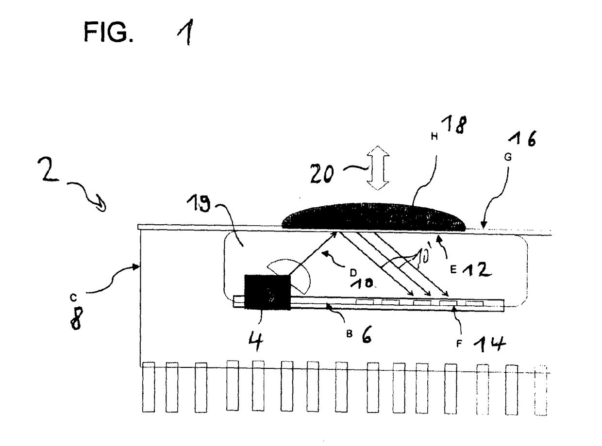
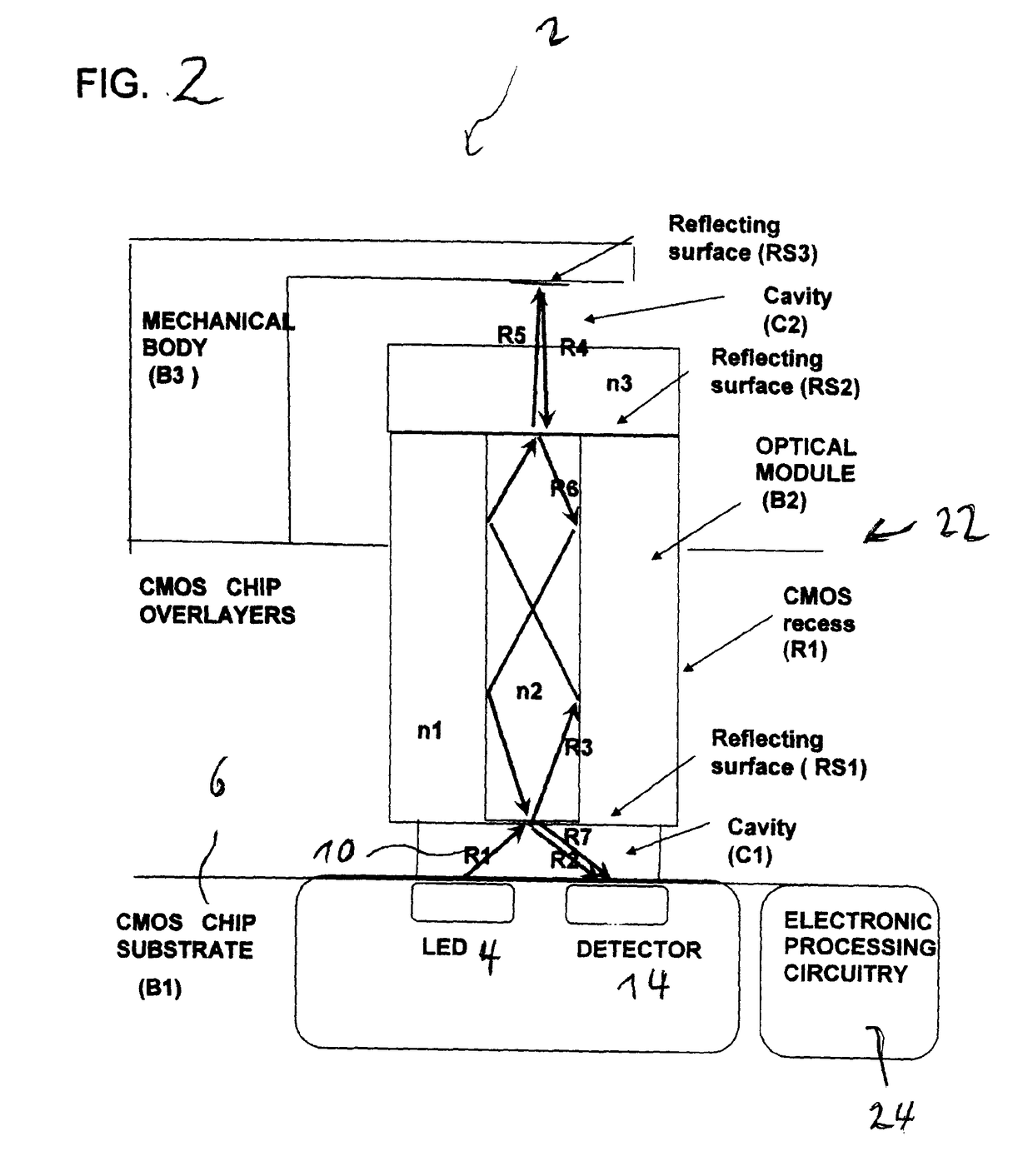
[0082]a micro photonic system 2 is outlined in FIG. 2. Using CMOS Integrated circuit with the integrated optical source 4 and directional emitter and detector structures 14 as a platform and adding some kind of optical-mechanical structure 22 in package form with which using the optical emissions 10 interact. Particular in this approach is the addition of an optical module 22 that accumulates light vertically from the chip 6 and waveguide light vertically outwards from the chip surface, collimates the optical radiation where it can subsequently interacts with secondary mechanical body and reflecting surface. Light is reflected vertically backwards into the module again, and is then wave-guided back onto the chip 6 surface. By controlling the positioning of the emitters 4 and detectors 14 relative to the module 22, the optical path of the transmitting and reflective components can be separated and the reflected component can be distinctively detected. The device 2 hence creates a sho...

first embodiment

[0194]In the invention as shown in FIG. 41, a micro RF oscillating and transmitting circuit and electronic driving and processing circuitry is fabricated on a printed circuit board platform using surface mount technology. The RF transmitting pattern is designed that is extremely wide angle or even omni-directional. The frequency is chosen to be in one of the permissible MHz or GHz bands. The dimensions of the total circuitry may in this case be bigger but it is envisaged that it will still be within credit card dimension limits. The RF transmitting pattern is designed that is extremely wide angle or even omni-directional. The frequency is chosen to be in one of the permissible MHz or GHz bands. The 2-20 GHz bands are particularly attractive since very small oscillating circuitry can be directly fabricated at micron dimensions on CMOS chip using lateral inductor and reverse bias capacitance or avalanche-capacitance technology. The transmitting carrier is appropriately modulated with ...

third embodiment

[0195]In the invention as shown in FIG. 42, a micro RF oscillating and transmitting circuit is fabricated on a CMOS chip platform. The RF transmitting pattern is designed that is extremely wide angle or even omni-directional. The frequency is chosen to be in one of the permissible MHz or GHz bands. The 2-20 GHz bands are particularly attractive since very small oscillating circuitry can be directly fabricated at micron dimensions on CMOS chip using lateral inductor and reverse bias capacitance or avalanche-capacitance technology. The transmitting carrier is appropriately modulated with on board CMOS modulation circuitry. Appropriate coding techniques can be used to transmit programmable and instructional information from the user card to the Master unit. The Master unit receives the information, can be coupled to secondary control circuitry. This unit can hence perform certain secondary tasks such identification of the user card and person, perform customized set up functions of a m...


PUM


Abstract

This invention relates to CMOS based micro-photonic systems comprising an optical source, means for optical transmission, and a detector, wherein the optical source is capable of emitting light having a wavelength being in a range in which a nitride comprising layer of said means for optical transmission is transparent and being below a detection threshold of said detector so as to enable the generation of a micro-photonic system in silicon integrated circuit technology.

Description

[0001]This invention relates to CMOS based micro-photonic systems[0002]Micro-photonic systems can be used in many CMOS based applications. For example, on-chip absorption, reflection, and fluorescence sensors, micro optical-electrical-mechanical sensors, mechanical sensor technology or optical communication systems are typical applications, which require light emitting diodes, light emitting lasers, optics, fiber optic technology, or mechanical sensor technology.[0003]The current chip based optical communication systems utilize discrete packages of group III-V and compound semiconductors that are fabricated in discrete packages and that is used in discrete form to build and compose optical fibre based optical communication systems.[0004]A vast majority of micro-electronic devices are formed in silicon. Over the last several decades, a substantial effort has been directed to refining the reliability and manufacturability of these devices. As a result, silicon-based microelectronic de...

Claims


Application Information

Patent Timeline
Patent Type & Authority Applications(United States)
IPC IPC(8): G02B6/122B81B7/00G02B6/14H04B10/50
CPCG02B6/122H04B10/501B81B7/0067G02B2006/12123G02B6/1225G02B2006/12035G02B6/14H04B10/801G02B6/43G02B6/136G01K11/00G01P5/20G01P5/26G01P15/093
Inventor SNYMAN, LUKAS WILLEM
Owner TSHWANE UNIV OF TECH
Why Eureka
Try Eureka