In situ tailoring of material properties in 3D printed electronics

Active Publication Date: 2017-10-19
UNIVERSITIES SPACE RES ASSOC
View PDF0 Cites 7 Cited by
  • Summary
  • Abstract
  • Description
  • Claims
  • Application Information

AI Technical Summary

Benefits of technology

[0010]Widely used screen printing technologies require pre and post processing for enhanced adhesion and tailoring the chemical state of the materials. Hence, there is a need for advanced printing technology for flexible electronics and 3D printed electronics that can tailor the physical, chemical and electronic properties of the materials being deposited.
[0028]There is further provided according to an embodiment of the invention a device wherein the inner and outer tubes of the print head nozzle has same or different thickness to enable sustaining of plasma in inner and outer region independently and enable materials to get accelerated towards the substrate with or without altering the material properties.
[0032]There is further provided according to an embodiment of the invention a device wherein the reproducibility of materials printing is ensured by reactive plasma jet cleaning of the nozzles by passing reactive gases and generating a plasma at significantly higher potential than the operating potential for printing so that the residues and contaminants formed during deposition are removed.

Problems solved by technology

In flexible electronics, the substrates vary from low glass transition temperature plastics to paper-like materials which cannot be efficiently used in well-established high vacuum based plasma deposition process.
However, in all these cases, tailoring the physical and chemical characteristics of the film requires additional post processing including thermal treatment and sometimes require an additional printing process.

Method used


Image

  • In situ tailoring of material properties in 3D printed electronics
  • In situ tailoring of material properties in 3D printed electronics
  • In situ tailoring of material properties in 3D printed electronics

Examples


Embodiment Construction

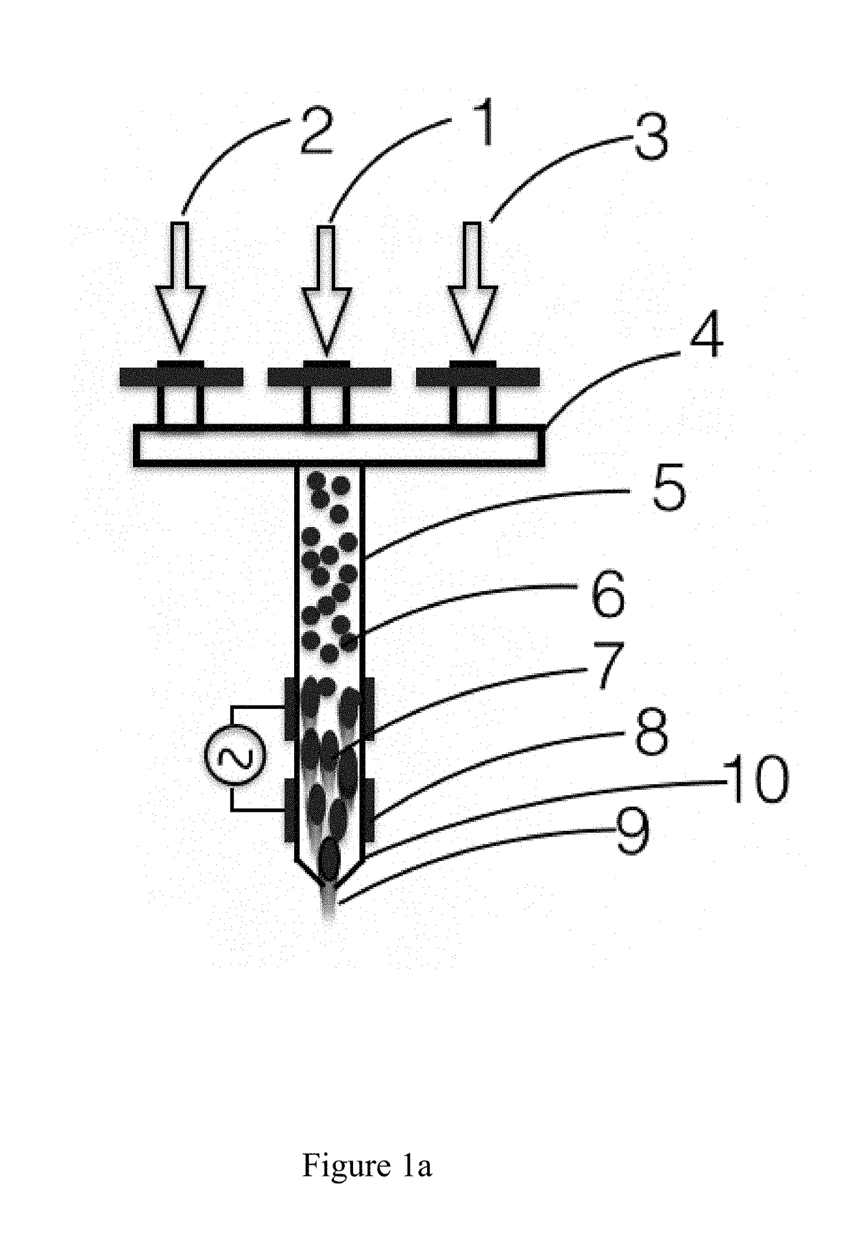
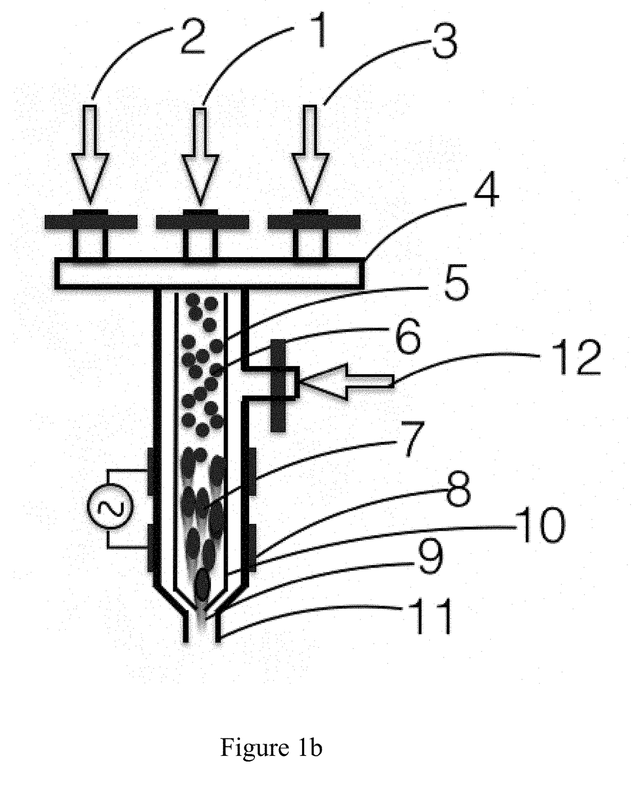
[0044]FIG. 1 shows the schematic of the plasma jet printer system with provisions for the addition of various process gases to tailor the material properties of the nanoparticle / microparticle in the plasma jet printer. Various process gases including helium, argon, hydrogen, nitrogen, carbon dioxide, oxygen, methane, alkane, alkene, silane, carbon tetra fluoride, sulfur hexafluoride, etc., can be used on their own or with appropriate mixture to suit the need. Nanoparticle / microparticle colloid input. FIG. 1 shows the following elements:[0045]Nanoparticle / microparticle colloid input 1[0046]Gas supply line for in situ processing 2[0047]Gas supply line for in situ processing 3[0048]Manifold for controlling the gas flow to the plasma jet nozzle 4[0049]Plasma jet printer nozzle 5[0050]Nanoparticle / microparticle colloid 6 in the plasma jet printer nozzle prior to exposure to plasma jet with particle size and shape same as the input colloid[0051]Nanoparticle / microparticle 7 in the plasma j...


PUM

PropertyMeasurementUnit
diameteraaaaaaaaaa
temperatureaaaaaaaaaa

Abstract

Systems and methods for highly reproducible and focused plasma jet printing and patterning of materials using appropriate ink containing aerosol through nozzles with narrow orifice and tubes with controlled dielectric constant connected to high voltage power supply, in the presence of electric field and plasma, that enables morphological and / or bulk chemical modification and / or surface chemical modification of the material in the aerosol and / or the substrate prior to printing, during printing and post printing.

Description

BACKGROUND OF THE INVENTIONField of the Invention[0001]This invention relates to the field of additive printing.Description of the Background[0002]There is a growing need for advanced metallization techniques for 3D interconnects in through silicon via (TSV) and 3D integration in integrated circuit (IC) packaging. There is also a demand for printing conductive patterns including printed circuit boards, interconnects, bumps in a range of substrates with varying glass transition temperature and outgassing properties.[0003]Flexible electronics, displays and wearable monitoring technologies require printing of conducting materials including conducting organics and / or metal coatings and interconnects on flexible and non-traditional substrates like plastics, cellulose, polymers, textiles where the conventional techniques for metallization are difficult to apply[0004]Printing of porous metal structures is critical for catalysis and it is routinely done using deposition on polymeric templat...

Claims


Application Information

Patent Timeline
Patent Type & Authority Applications(United States)
IPC IPC(8): C23C16/513C23C16/52B33Y10/00B33Y30/00
CPCC23C16/513B33Y30/00B33Y10/00C23C16/52C23C16/4401H05H1/2406H05H1/42H05H1/246
Inventor GANDHIRAMAN, RAMPRASADMEYYAPPAN, MEYYAKOEHNE, JESSICA E.
Owner UNIVERSITIES SPACE RES ASSOC
Why Eureka
Try Eureka