Semiconductor device and method for manufacturing semiconductor device

a semiconductor and semiconductor technology, applied in the direction of printed circuit manufacturing, printed circuit aspects, printed element electric connection formation, etc., can solve the problem that the heat dissipation properties cannot be maintained for a required lifetime, and achieve satisfactory heat dissipation properties and reduce metal fatigue of the bonding member

Active Publication Date: 2017-10-26
MITSUBISHI ELECTRIC CORP
View PDF9 Cites 16 Cited by
  • Summary
  • Abstract
  • Description
  • Claims
  • Application Information

AI Technical Summary

Benefits of technology

[0011]A semiconductor device according to one aspect of the present techniques includes: an insulating substrate including an insulating plate and conductive plates which are provided on opposite surfaces of the insulating plate; a semiconductor chip provided on an upper surface of the insulating substrate; a plate member bonded to a lower surface of the insulating substrate; and a cooler bonded to a lower surface of the plate member, wherein at least one of bonding between the lower surface of the insulating substrate and the plate member and bonding between the lower surface of the plate member and the cooler is performed via a bonding member which is composed mainly of tin, and a cyclic stress of the plate member is smaller than a tensile strength of the bonding member.
[0012]A method for manufacturing a semiconductor device according to one aspect of the present techniques includes: bonding an upper surface of an insulating substrate which includes an insulating plate and conductive plates which are provided on opposite surfaces of the insulating plate, to a semiconductor chip; bonding a lower surface of the insulating substrate and a plate member; and bonding a lower surface of the plate member and a cooler, wherein at least one of bonding between the lower surface of the insulating substrate and the plate member and bonding between the lower surface of the plate member and the cooler is performed via a bonding member which is composed mainly of tin, a cyclic stress of the plate member is smaller than a tensile strength of the bonding member, and a temperature at which bonding is performed via the bonding member is lower than a temperature at which the upper surface of the insulating substrate is bonded to the semiconductor chip.
[0014]Because of the foregoing configuration, since the cyclic stress of the plate member is smaller than the tensile strength of the bonding member, it is possible to reduce metal fatigue of the bonding member which is induced by a thermal stress caused due to a difference in a thermal expansion coefficient, while maintaining satisfactory heat transfer properties.
[0017]The objects, features, aspects and advantages of the present techniques will become more apparent from the following detailed description when taken in conjunction with the accompanying drawings.

Problems solved by technology

However, depending on a use condition, a thermal stress is caused due to a difference in thermal expansion coefficient between the insulating substrate and the cooler, and a crack occurs in a bonding member which bonds the insulating substrate and the cooler, so that satisfactory heat dissipation properties cannot be maintained throughout a required lifetime in some cases.

Method used


Image

  • Semiconductor device and method for manufacturing semiconductor device
  • Semiconductor device and method for manufacturing semiconductor device
  • Semiconductor device and method for manufacturing semiconductor device

Examples


first embodiment

Configuration

[0047]Below, in portions where symbols of elements or names of materials such as copper (Cu) or aluminum (Al) are described without specific statements, elements or materials including other additives such as a copper alloy or an aluminum alloy, for example, shall be included.

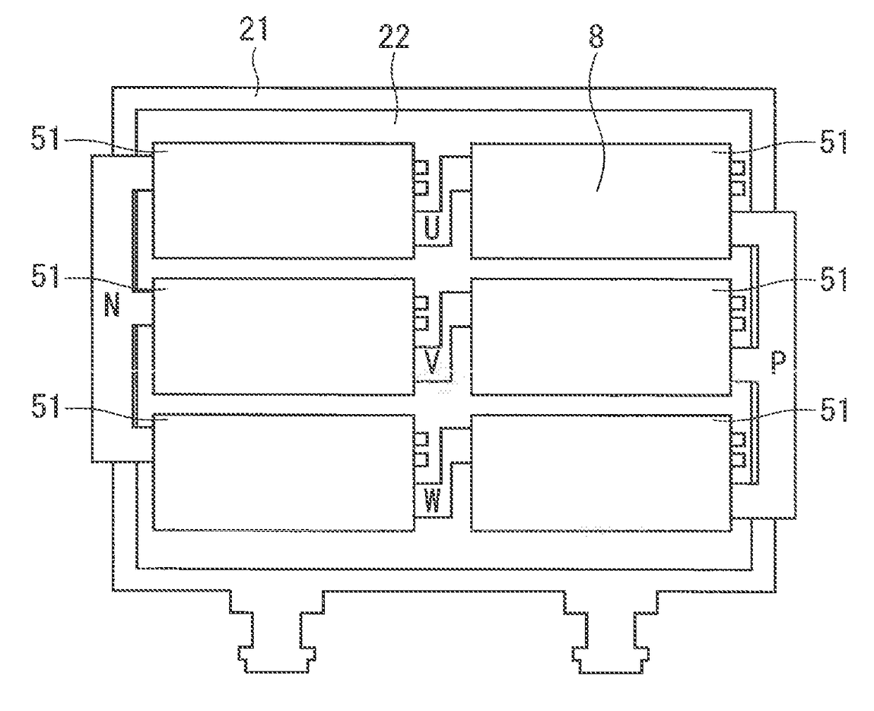
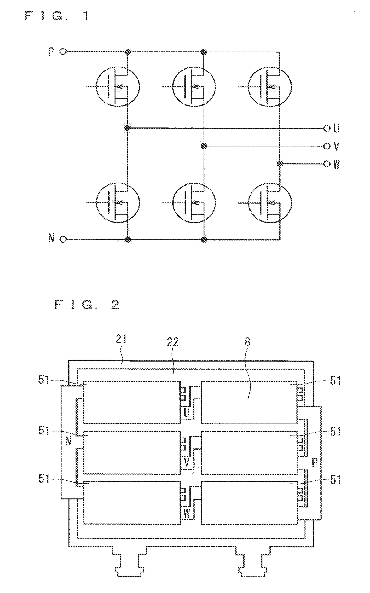
[0048]FIG. 1 is a circuit diagram of a power module for a three-phase inverter using a MOSFET as one example of a semiconductor device regarding the present embodiment. Also, FIG. 2 is a top view of the power module regarding the present embodiment in a case where the power module is formed of one-in-one submodules (one arm is provided per submodule). In this regard, while an arm is a unit corresponding to one MOSFET serving as a semiconductor element in a case illustratively shown in FIG. 1, an arm corresponds to a plurality of MOSFETs in a case where a plurality of MOSFETs are connected in parallel to serve as switching elements, for example. Also, in a case of an IGBT, for example, an arm corres...

second embodiment

Manufacturing Method

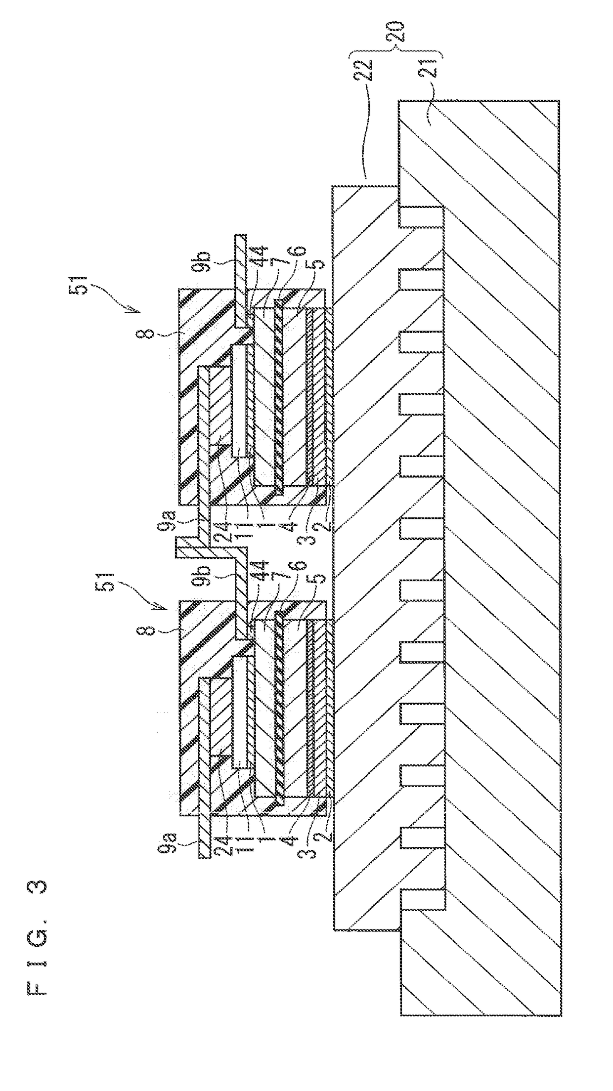
[0092]Next, as a second example of a manufacturing method, a manufacturing method for a case where the bonding member 2 is a Cu-Sn alloy obtained by liquid phase diffusion bonding and the laminated plate member 33 is bonded to the cooler 20, will be described with reference to FIG. 18 through FIG. 22.

[0093]As illustratively shown in FIG. 18, a so-called die-bonding step in which the semiconductor chip 11 is bonded to the insulating substrate 13 is performed. The bonding member 1 is prepared such that a melting point or a solidus thereof is higher than the highest temperature reached by the bonding member 1 in a soldering step in which soldering is performed, in order to prevent the bonding member 1 from melting when being soldered in a later step. This requirement is satisfied by a so-called Ag sintering process using a silver nanoparticle, the above-described liquid phase diffusion process, or high melting-point solder, for example. Among those processes, an Ag ...

third embodiment

[0100]Next, as a third example of a manufacturing method, description will be made about a case where the bonding member 4 is formed of the same material as the bonding member 2. A method for manufacturing the submodule 51 is similar to the example of manufacturing method described in the second embodiment.

[0101]The bonding member 2, the laminated plate member 33, and the bonding member 4 are placed in the stated order from the top, between the submodule 51 and the cooler 20, and those members are simultaneously bonded using a reflow furnace or the like. While a completed configuration is similar to the configuration illustratively shown in FIG. 22, the bonding member 2 and the bonding member 4 are formed of the same material and thus need not be dealt with as distinguished from each other.

[0102]In the case of the third embodiment, a bonding step using the bonding member 4 can be omitted as compared to the manufacturing method described in the first embodiment and the manufacturing ...


PUM


Abstract

A semiconductor device and a method for manufacturing the semiconductor device. The semiconductor device includes an insulating substrate, a semiconductor chip, a plate member, and a cooler. The insulating substrate includes insulating ceramics serving as an insulating plate, and conductive plates provided on opposite surfaces of the insulating ceramics. The semiconductor chip is provided on an upper surface of the insulating substrate. The plate member is bonded to a lower surface of the insulating substrate. The cooler is bonded to a lower surface of the plate member. At least one of bonding between a lower surface of the insulating substrate and the plate member and bonding between a lower surface of the plate member and the cooler is performed via a bonding member composed mainly of tin. Also, a cyclic stress of the plate member is smaller than a tensile strength of the bonding member.

Description

TECHNICAL FIELD[0001]The present techniques relate to a semiconductor device and a method for manufacturing a semiconductor device, and particularly relate to a semiconductor device which is required to have heat dissipation properties, and a method for manufacturing such a semiconductor device.BACKGROUND ART[0002]In a semiconductor device (power module) which uses a power semiconductor chip such as a silicon-carbide metal oxide semiconductor-field effect transistor (SiC MOSFET) or a silicon insulated gate bipolar transistor (Si IGBT), there is a need to efficiently dissipate heat generated from a semiconductor chip, and keep a temperature of a semiconductor chip at a predetermined temperature or lower.[0003]Conventionally, provided is a power module in which a semiconductor chip is bonded to one of surfaces of a so-called insulating substrate which is formed by integration of: an insulating ceramic plate of high thermal conductivity such as silicon nitride, silicon aluminum, or alu...

Claims


Application Information

Patent Timeline
Patent Type & Authority Applications(United States)
IPC IPC(8): H01L23/473H01L23/367H05K3/00H05K3/34H01L23/373H05K1/03H05K3/40
CPCH01L23/473H05K3/0061H01L23/367H05K3/341H01L23/3677H05K3/4015H01L2924/0002H05K1/0306H05K2201/0373H05K2201/09681H05K2201/0969H01L23/3735H01L2924/181H01L2224/73265H01L2224/92247H01L23/36H01L23/4334H01L23/49811H01L21/4882H01L2224/32225H01L2224/48247H01L2924/00014H01L2224/3303H01L24/29H01L24/32H01L24/33H01L24/45H01L24/48H01L24/73H01L24/83H01L24/92H01L2224/29111H01L2224/2929H01L2224/29339H01L2224/32245H01L2224/33181H01L2224/45124H01L2224/48091H01L2224/73215H01L2224/8384H01L2224/92246H01L2924/10272H01L2924/13055H01L2924/13091H01L25/115H01L2924/00012H01L2224/45099H01L2924/01029H01L2924/00
Inventor KOBAYASHISODA, SHINNOSUKEOMOTO, YOHEIHAYASHI, KOMEI
Owner MITSUBISHI ELECTRIC CORP
Why Eureka
Try Eureka