Composition for forming hole collecting layer of photosensor element, and photosensor element

a technology of photosensor elements and collecting layers, which is applied in the direction of coatings, solid-state devices, semiconductor devices, etc., can solve the problems of accelerating device deterioration, high equipment cost, and high equipment cost, and achieves low dark current, high photoelectric conversion efficiency, and high uniform film formability.

Active Publication Date: 2018-04-26
NISSAN CHEM IND LTD
View PDF3 Cites 0 Cited by
  • Summary
  • Abstract
  • Description
  • Claims
  • Application Information

AI Technical Summary

Benefits of technology

[0026]By using the inventive composition for forming a hole-collecting layer of a photosensor element, a photosensor element that achieves both a high photoelectric conversion efficiency and a low dark current can be obtained.
[0027]Also, because the inventive composition is a uniform organic solution, it is highly compatible with mass production processes. Moreover, because it exhibits a high uniform film formability while planarizing the underlying anode having surface irregularities, a high device yield can be achieved.
[0028]Finally, the hole-collecting layer created from the inventive composition exhibits a high heat resistance, and thus can withstand various high-temperature processes following film formation.
[0029]The invention is described in greater detail below.
[0030]The inventive composition for forming a hole-collecting layer of a photosensor element includes a charge-transporting substance having a molecular weight of from 200 to 2,000 and an organic solvent.
[0031]Although the molecular weight of the charge-transporting substance used in the invention is from 200 to 2,000, taking into account the electrical conductivity, the lower limit is preferably 300 or more, and more preferably 400 or more. From the standpoint of increasing the solubility in solvents, the upper limit is preferably 1,500 or less, and more preferably 1,000 or less.

Problems solved by technology

However, vacuum deposition has drawbacks in terms of, for example, its complexity as a mass production process, the high cost of the equipment, and the efficiency of material utilization.
However, because these are aqueous dispersions, the complete removal of moisture and the control of moisture reabsorption are difficult, which tends to accelerate device deterioration.
Moreover, there remain a variety of challenges facing the use of aqueous dispersions of PEDOT / PSS in mass production.
Namely, because such dispersions are prone to solids agglomeration, defects readily arise in applied films made thereof and the coating equipment has a tendency to clog or corrode, in addition to which the applied films leave something to be desired in terms of heat resistance.
Although applying an external electrical field is likely to improve the light-receiving sensitivity and the response speed, the injection of holes and electrons from the electrodes arises, resulting in an increase in the dark current.

Method used


Image

  • Composition for forming hole collecting layer of photosensor element, and photosensor element
  • Composition for forming hole collecting layer of photosensor element, and photosensor element
  • Composition for forming hole collecting layer of photosensor element, and photosensor element

Examples


preparation example 1

[0133]Chlorobenzene (2.0 mL) was added to a sample vial containing 20 mg of PTB7 (available from 1-Material) and 30 mg of PC61BM (available from Frontier Carbon Corporation under the product name “nanom spectra E100”), and the vial contents were stirred for 15 hours on a hot plate set to 80° C. The resulting solution was then allowed to cool to room temperature, following which 60 μL of 1,8-diiodooctane (Tokyo Chemical Industry Co., Ltd.) was added and stirring was carried out, giving Solution A1 (a photoelectric conversion layer-forming composition).

[2] Preparation of Silane Solution

preparation example 2

[0134]Silane Compound Solution S1 was obtained by adding 0.717 mg (3.61 mmol) of phenyltrimethoxysilane (Shin-Etsu Chemical Co., Ltd.) and 0.394 mg (1.81 mmol) of 3,3,3-trifluoropropyltrimethoxysilane (Shin-Etsu Chemical Co., Ltd.) to 10.0 g of N,N-dimethylacetamide (DMAc) and stirring at room temperature.

[3] Preparation of Hole-Collecting Layer-Forming Compositions

working example 1-1

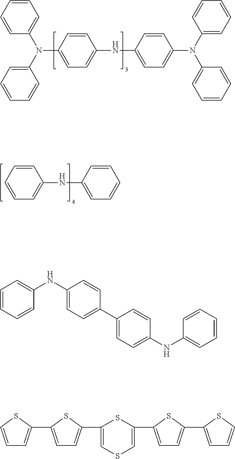
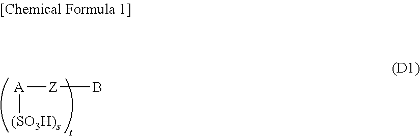
[0135]DMAc (3.33 g) and 2,3-butanediol (1.67 g) were added to a mixture of 67.1 mg (0.152 mmol) of the phenyltetraaniline of formula (d) above and 136.9 mg (0.152 mmol) of the arylsulfonic acid compound of above formula (D2) that was synthesized according to the method described in WO 2006 / 025342 (the same applies below), and the solids were dissolved by stirring at room temperature under ultrasonic irradiation. To this was added 5.0 g of cyclohexanol (CHN) and stirring was carried out, giving a light green-colored solution. The resulting light green-colored solution was filtered with a syringe filter having a pore size of 0.2 μm, giving Hole-Collecting Layer-Forming Composition B1.

[0136]The phenyltetraaniline of formula (d) above was synthesized according to the method described in Bulletin of Chemical Society of Japan, Vol. 67, pp. 1749-1752 (1994).


PUM

PropertyMeasurementUnit
boiling pointaaaaaaaaaa
viscosityaaaaaaaaaa

Abstract

A photosensor element that is capable of achieving a good balance between high photoelectric conversion efficiency and low dark current is able to be obtained by using a composition for forming a hole collecting layer of a photosensor element, which contains an organic solvent and a charge-transporting material that is composed, for example, of an aniline derivative or thiophene derivative represented by one of formulae (AA)-(DD) and having a molecular weight of 200-2,000.

Description

TECHNICAL FIELD[0001]The present invention relates to a composition for forming a hole-collecting layer of a photosensor element, and a photosensor element.BACKGROUND ART[0002]Photoelectron multipliers which utilize the photoelectric effect and photodiodes which utilize pn junctions have hitherto been used as photosensors. Such photosensors are employed in a broad range of applications that include not only light sensing, but also, as solid-state imaging devices, image sensors for civilian use and on-board applications in vehicles.[0003]Lately, given current trends toward smaller sizes and lighter weights, and also the importance placed on low cost and decorative design, organic photosensors that use organic materials in the photoelectric conversion layers are being developed and have been attracting attention.[0004]Organic photosensors are constructed of, for example, a photoelectric conversion layer, charge (hole, electron) collecting layers, electrodes (anode, cathode) and an opt...

Claims


Application Information

Patent Timeline
Patent Type & Authority Applications(United States)
IPC IPC(8): H01L51/00
CPCH01L51/0059H01L51/0036H01L51/0047H01L51/0068H01L51/0035H01L51/42H01L27/14643C08G61/122C08G61/126C08G2261/3223C09D179/02C08G73/0266C08K3/045Y02E10/549H10K71/15H10K85/111H10K85/215H10K85/151H10K85/113H10K85/626H10K85/615H10K30/81H10K30/30C08L65/00C08K5/42H10K85/633H10K30/00H10K85/631H10K85/655C08G73/00
Inventor OSHIMA, JUROYOSHIMOTO, TAKUJI
Owner NISSAN CHEM IND LTD
Why Eureka
Try Eureka