

Screen-printable boron doping paste with simultaneous inhibition of phosphorus diffusion in co-diffusion processes
a technology of phosphorus diffusion and co-diffusion, which is applied in the direction of crystal growth process, sustainable manufacturing/processing, final product manufacturing, etc., can solve the problems of not having major industrial importance, not completely suppressing phosphorus diffusion on the back, and hardly still using the etching technique in industrial practi
- Summary
- Abstract
- Description
- Claims
- Application Information
AI Technical Summary
Benefits of technology
Problems solved by technology
Method used
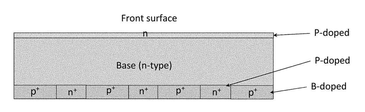
Image

Examples
example 1
[0108]8 g of boron oxide were initially introduced in a glass flask and suspended in 80 g of acetic anhydride and 160 g of tetrahydrofuran. The mixture was brought to reflux, and 24.2 g of ethylene glycol monobutyl ether (EGB) were added. 24.2 g of diethoxydimethylsilane and 31 g of dimethyldimethoxysilane were subsequently added to the refluxing mixture, and this was warmed with boiling for 30 minutes. A solution consisting of 480 g of EGB and 250 g of Texanol, in which 2.5 g of water, 2 g of 1,3-cyclohexanedione and 4.2 g of acetaldoxime were dissolved, was added to the siloxane-containing solution and allowed to mix for 20 minutes. Over the same period, the reaction temperature was increased from 80° C. to 120° C. After the mixing, 50 g of aluminium tri-sec-butylate, dissolved in 400 g of dibenzyl ether, were allowed to run into the reaction mixture over the course of five minutes, and the completed mixture was left to react for a further 55 minutes. The reaction mixture was then...
example 2
[0109]A paste in accordance with Example 1, characterised by a mass proportion of 4.3% of ethylcellulose, was printed onto a silicon wafer surface using a 350 mesh screen having a wire diameter of 16 μm, an emulsion thickness of 8 μm to 12 μm, and furthermore using a squeegee speed of 200 mm / s and a squeegee pressure of 1 bar, and subsequently subjected to drying in a through-flow oven using the following heating zone temperatures: 350 / 350 / 375 / 375 / 375 / 400 / 400° C.
[0110]Paste mixtures having a mass proportion of greater than 5% and also those having a mass proportion of less than 2.5% cannot be processed by means of the screen printing process.
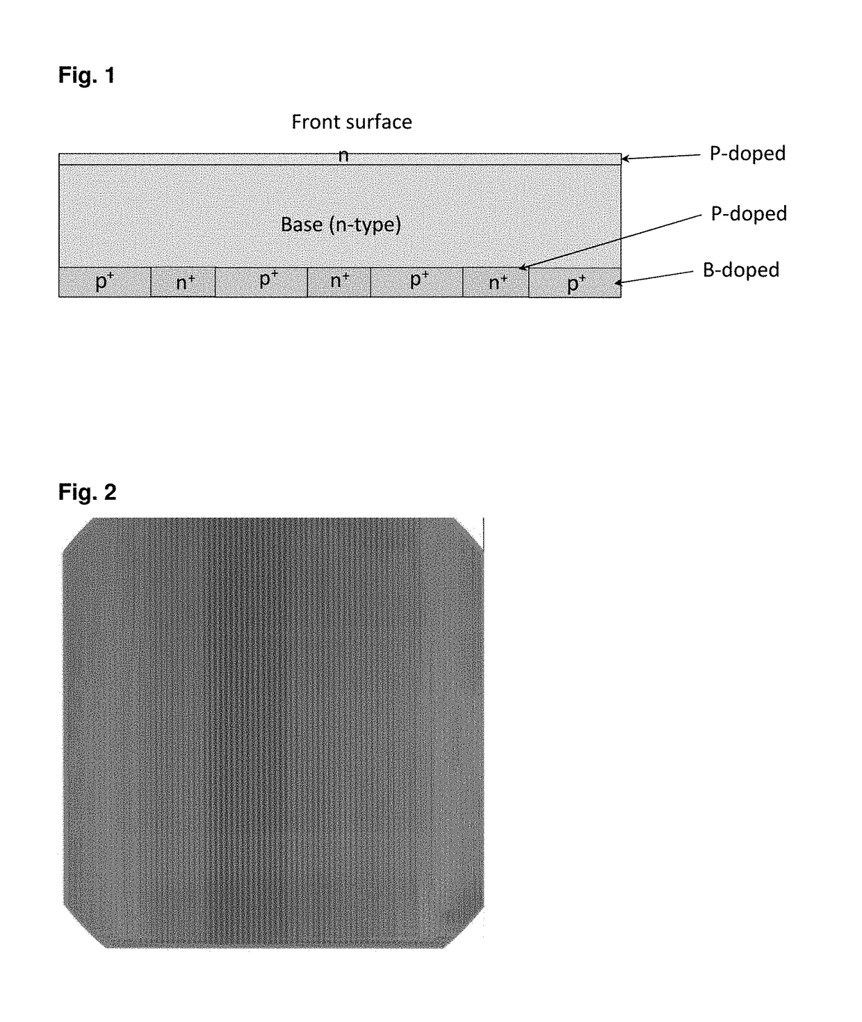
[0111]FIG. 2: shows a silicon wafer printed with the aid of a boron-containing doping paste according to the invention and in accordance with the composition and preparation of Example 1, after drying in a through-flow oven. The different colours (→ interference colours) correspond to differences in locally present glass film thicknesses. Optimi...
example 3
[0112]4 g of boron oxide were initially introduced in a glass flask and suspended in 40 g of acetic anhydride and 80 g of tetrahydrofuran. The mixture was brought to reflux, and 11.25 g of ethylene glycol monobutyl ether (EGB) were added. 12.1 g of diethoxydimethylsilane and 15.1 g of dimethyldimethoxysilane were subsequently added to the refluxing mixture, and this was warmed with boiling for 30 minutes. 32.5 g of the siloxane-containing solution were mixed with 69.8 g of a solution consisting of 240 g of EGB and 125 g of Texanol, and the heating temperature was increased from 80° C. to 120° C. over the course of 20 minutes with stirring of the reaction mixture. 1.75 g of 1,3-cyclohexanedione, 0.75 g of acetaldoxime and 0.5 g of water were dissolved in the reaction mixture. 10 g of aluminium tri-sec-butylate dissolved in 40 g of dibenzyl ether were subsequently added dropwise to the reaction mixture over the course of five minutes. After the addition, the mixture was left to react ...
PUM
| Property | Measurement | Unit |
|---|---|---|
| temperatures | aaaaa | aaaaa |
| temperatures | aaaaa | aaaaa |
| temperatures | aaaaa | aaaaa |
Abstract
Description
Claims
Application Information