

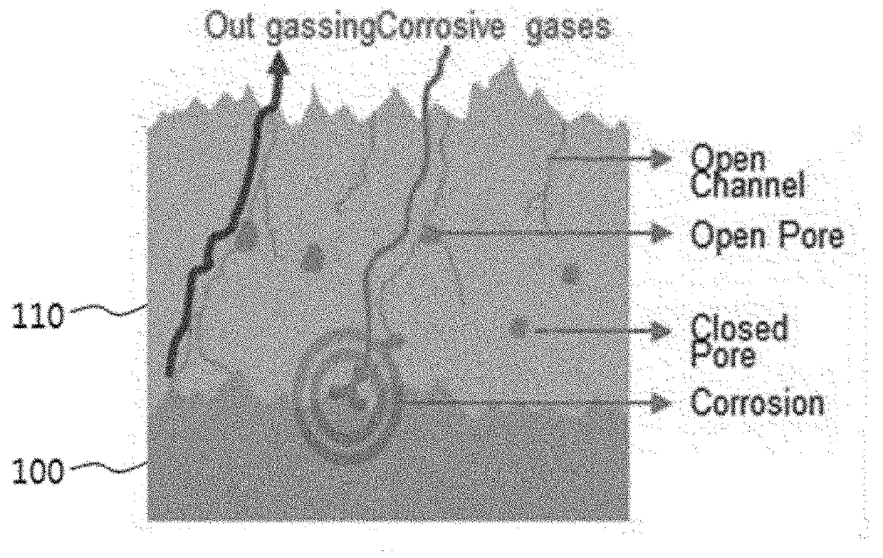
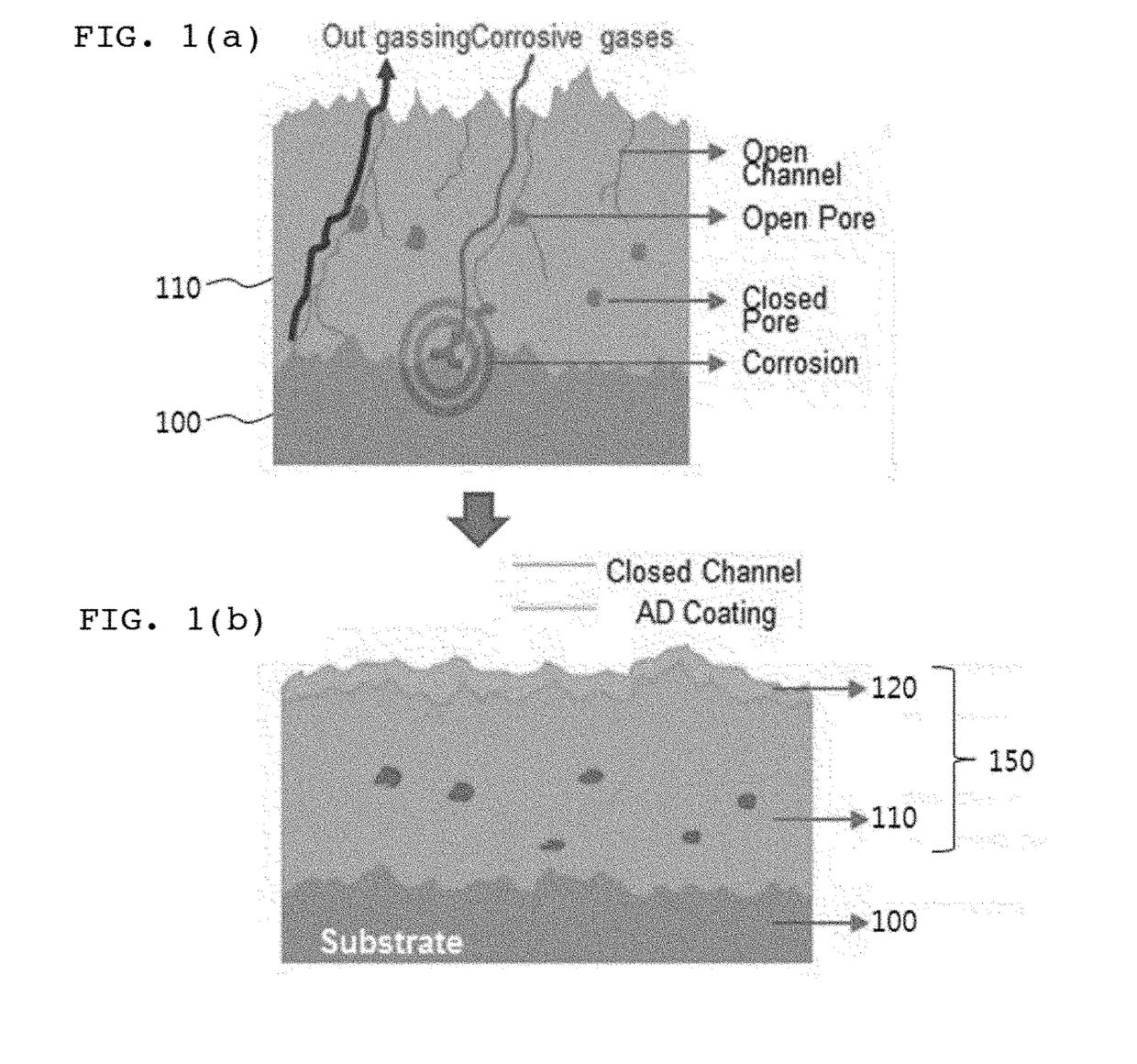
Plasma resistant coating film and fabricating method thereof
a technology of coating film and coating layer, which is applied in the direction of coating, rare earth metal fluoride, yittrium oxide/hydroxide, etc., can solve the problems of difficult to develop high binding force between the coating layer and the matrix, lack of economic feasibility, and excessive processing time, so as to improve the physical properties of the coating layer and increase the binding force. , the effect of high electrical resistan
- Summary
- Abstract
- Description
- Claims
- Application Information
AI Technical Summary
Benefits of technology
Problems solved by technology
Method used
Image

Examples
embodiment 1
1-1: Forming the First Rare Earth Metal Compound Layer
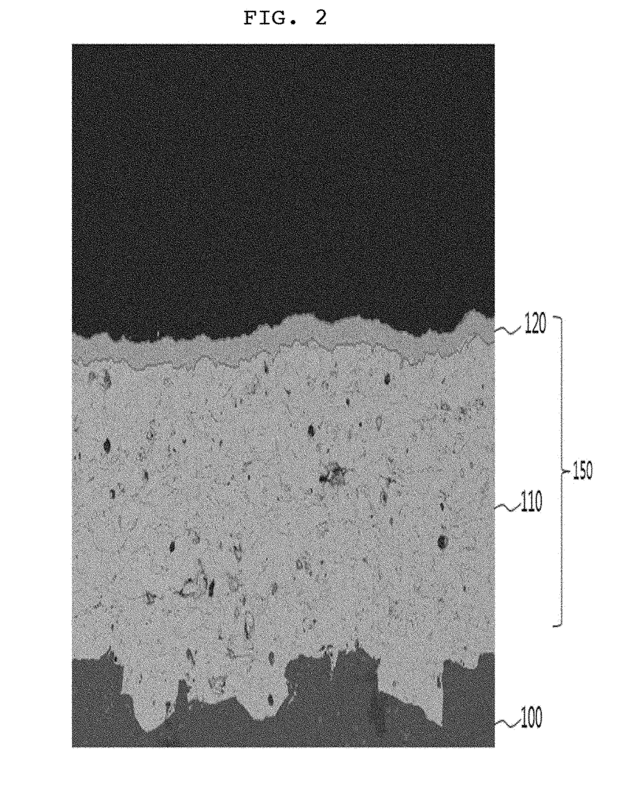
[0085]The first rare earth metal compound layer with a thickness of 150 μm was formed by thermal spraying yttria (Y2O3) particles for thermal spray coating with an average grain size of 30 μm on an aluminum plate of 5 cm×5 cm×0.5 cm by using the plasma spray coating technique (He and Ar as process gas, heat source of 3000 K).
1-2: Forming the Second Rare Earth Metal Compound Layer
[0086]The second rare earth metal compound layer with a thickness of 10 μm was formed by aerosolizing yttria (Y2O3) particles by using a particle vibrator in an aerosol chamber maintained in vacuum atmosphere at ambient temperature and then physically colliding at about 300 m / s the aerosolized yttria particles together with Ar gas onto the first rare earth metal compound layer of the Embodiment 1-1 by using the pressure difference between the aerosol chamber and a deposition chamber.
1-3: Fabricating the Coating Film
[0087]The aluminum pate on which the sec...
embodiment 2
[0090]The plasma resistant coating film was fabricated according to the same method as employed in the Embodiment 1 with the addition of the second rare earth metal compound layer formed by using YOF particles.
experimental example 1
[0100]Surface roughness values (μm) of the coating films fabricated in the Embodiments and the Comparative Examples of the present disclosure were measured with a roughness measuring device (SJ-201), whose results are listed in Table 1.
TABLE 1Surface roughness (μm)The first rare earthThe second rare earthmetal compound layermetal compound layerEmbodiment 12.52.8Embodiment 22.72.7Comparative Ex. 12.52.9Comparative Ex. 22.52.8Comparative Ex. 42.72.8Comparative Ex. 52.72.8
[0101]As shown in Table 1, the surface roughness did not change after the wetting treatment.
PUM
| Property | Measurement | Unit |
|---|---|---|
| thickness | aaaaa | aaaaa |
| thickness | aaaaa | aaaaa |
| surface roughness | aaaaa | aaaaa |
Abstract
Description
Claims
Application Information