
Organic light emitting display

Active Publication Date: 2018-06-07
SAMSUNG SDI CO LTD
View PDF1 Cites 8 Cited by
  • Summary
  • Abstract
  • Description
  • Claims
  • Application Information

AI Technical Summary

Benefits of technology

The present invention provides an organic light emitting diode display apparatus with several technical benefits. First, it includes an organic layer with high plasma resistance, which ensures better performance and reliability of the display. Second, it has low water vapor permeability and oxygen permeability, which means that the organic layer is less likely to get damaged by surrounding moisture and gas. Third, it is transparent and has low surface roughness, which makes it easy to use and provides a smooth display surface. Finally, it includes an organic layer that is more vulnerable to moisture and oxygen, which is formed so as not to be exposed at the edge of the encapsulation layer, thus improving reliability in elapsed time.

Problems solved by technology

Organic light emitting diodes are vulnerable to moisture and / or gas.
Organic light emitting diodes can suffer from delamination at an interface between a metal field and a light emitting layer due to moisture.
The organic light emitting diodes can have high resistance due to oxidation of metals and can suffer from degradation of organic materials in the light emitting layer due to moisture and / or oxygen.
The organic light emitting diode can suffer from deterioration in light emission due to oxidation of the light emitting layer or the metal field by outgassing inside or outside the organic light emitting diodes.
Etching of the organic layers can deteriorate an encapsulation function of the organic layers and provide adverse influence on formation of the inorganic layers.
If the organic layers exhibit low resistance to plasma, there can be difficulty in formation of the inorganic layers.
As a result, the organic light emitting diode can suffer from deterioration in luminous characteristics and reliability.
Thus, the encapsulation layer can suffer from slight lifting between the inorganic layers and / or delamination or slight lifting between the substrate and the inorganic layer.
As a result, the inorganic layers cannot sufficiently prevent moisture and / or oxygen from penetrating the organic light emitting diode.

Method used


Image

  • Organic light emitting display
  • Organic light emitting display
  • Organic light emitting display

Examples


example 2

Preparative Example 2

[0145]In a 2000 ml flask provided with a cooling tube and a stirrer, 600 ml of dichloromethane (Sigma Aldrich Co., Ltd.), 58.8 g of 2-hydroxyethyl methacrylate (Sigma Aldrich Co., Ltd) and 52.2 g of trimethylamine (Sigma Aldrich Co., Ltd.) were placed, followed by stirring at 0° C. while slowly adding 100 g of triphenyl chloromethane (Sigma Aldrich Co., Ltd.). The flask was heated to 25° C., followed by stirring for 4 hours. Then, dichloromethane was removed through distillation, followed by performing silica gel column chromatography, thereby obtaining 124 g of a compound represented by Formula 6. The obtained compound had an HPLC purity of 97%.

example 3

Preparative Example 3

[0146]In a 2000 ml flask provided with a cooling tube and a stirrer, 800 ml of acetonitrile (Fisher Co., Ltd.), 180 g of potassium carbonate (Aldrich Co., Ltd), and 108 g of acrylic acid were placed, followed by stirring at 0° C. while slowly adding 150 g of 4,4′-bis(chloromethyl) biphenyl (TCI Co., Ltd.). The flask was heated to 70° C., followed by stirring for 12 hours. Then, acetonitrile was removed through distillation, followed by performing silica gel column chromatography, thereby obtaining 177 g of a compound represented by Formula 7. The obtained compound had an HPLC purity of 97%.

example 4

Preparative Example 4

[0147]In a 3000 ml flask provided with a cooling tube and a stirrer, 300 ml of dichloromethane (Sigma Aldrich Co. Ltd.), 200 g of 2-hydroxyethyl acrylate (Shin Nakamura Chemical Co., Ltd.), and 168 g of triethylamine were placed, followed by cooling the flask to 0° C. and stirring for 2 hours while dropwise adding a solution obtained by dissolving 278 g of p-toluene sulfonyl chloride (Sigma Aldrich Co. Ltd.) in 500 ml of dichloromethane thereto. After additional stirring for 5 hours, residual solvents were removed by distillation. 300 g of the obtained compound was placed into 1000 ml of acetonitrile (Sigma Aldrich Co. Ltd.), and then 220 g of potassium carbonate (Aldrich Co., Ltd.) and 141 g of 2-phenyl phenol (Sigma Aldrich Co. Ltd.) were added thereto, followed by stirring at 80° C. Residual solvents and reaction residues were removed, thereby obtaining a compound represented by Formula 8. The obtained compound (weight average molecular weight: 296.36) had an...


PUM

PropertyMeasurementUnit
Thicknessaaaaaaaaaa
Thicknessaaaaaaaaaa
Molar massaaaaaaaaaa

Abstract

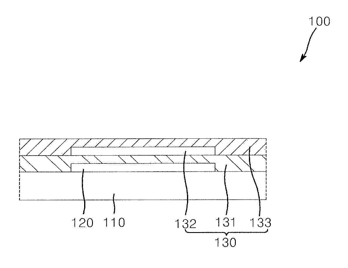
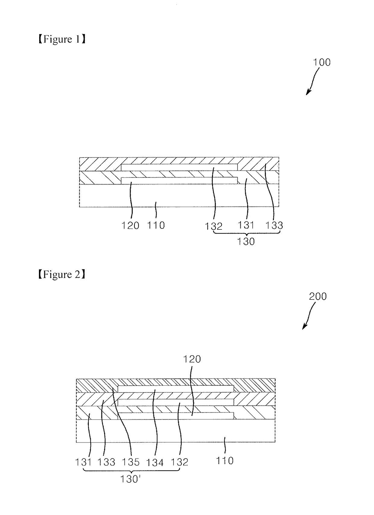
Disclosed is an organic light emitting diode display apparatus including: a substrate; an organic light emitting diode disposed on the substrate; and an encapsulation layer encapsulating the organic light emitting diode. The encapsulation layer has a structure in which two or more inorganic layers and one or more organic layers are alternately stacked one above another, two adjacent inorganic layers at least partially contact each other, and the organic layers are formed of an encapsulating composition. The encapsulating composition includes a photocurable monomer and a photopolymerization initiator. The photocurable monomer includes a monomer containing no aromatic hydrocarbon group; and a monomer having two or more substituted or unsubstituted phenyl groups represented by Formula 1. The photocurable monomer includes about 5 wt % to about 45 wt % of the monomer having two or more substituted or unsubstituted phenyl groups and about 55 wt % to about 95 wt % of the monomer containing no aromatic hydrocarbon group.

Description

TECHNICAL FIELD[0001]The present invention relates to an organic light emitting diode display apparatus.BACKGROUND ART[0002]Organic light emitting diodes are vulnerable to moisture and / or gas. Organic light emitting diodes can suffer from delamination at an interface between a metal field and a light emitting layer due to moisture. The organic light emitting diodes can have high resistance due to oxidation of metals and can suffer from degradation of organic materials in the light emitting layer due to moisture and / or oxygen. The organic light emitting diode can suffer from deterioration in light emission due to oxidation of the light emitting layer or the metal field by outgassing inside or outside the organic light emitting diodes. Thus, the organic light emitting diode must be encapsulated by an encapsulation composition capable of protecting the organic light emitting diode from moisture and / or gas.[0003]The organic light emitting diode can be encapsulated by an encapsulation la...

Claims


Application Information

Patent Timeline
IPC IPC(8): H01L27/32H01L51/52
CPCH01L27/3209H01L51/5237H01L27/3297H10K59/131H10K59/8731B32B27/08H01L23/293H10K50/8445H10K50/84H10K50/85H10K59/32
Inventor KIM, HYE JINKO, SUNG MINKIM, MI SUNNAM, SEONG RYONGLEE, JI YEONCHOI, MI JEONG
Owner SAMSUNG SDI CO LTD
Learn More