

Organic electron transport material
- Summary
- Abstract
- Description
- Claims
- Application Information
AI Technical Summary
Benefits of technology
Problems solved by technology
Method used
Image

Examples
example 1
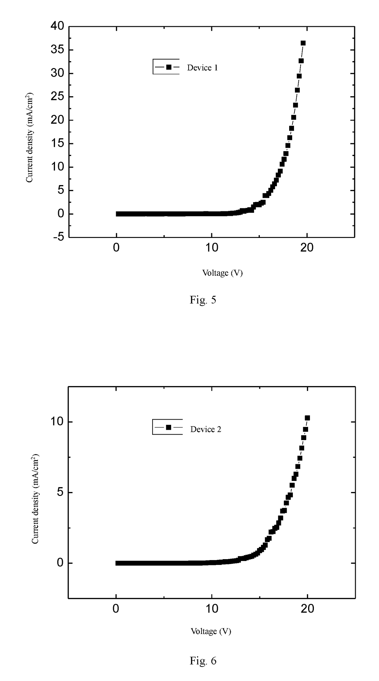
[0033]
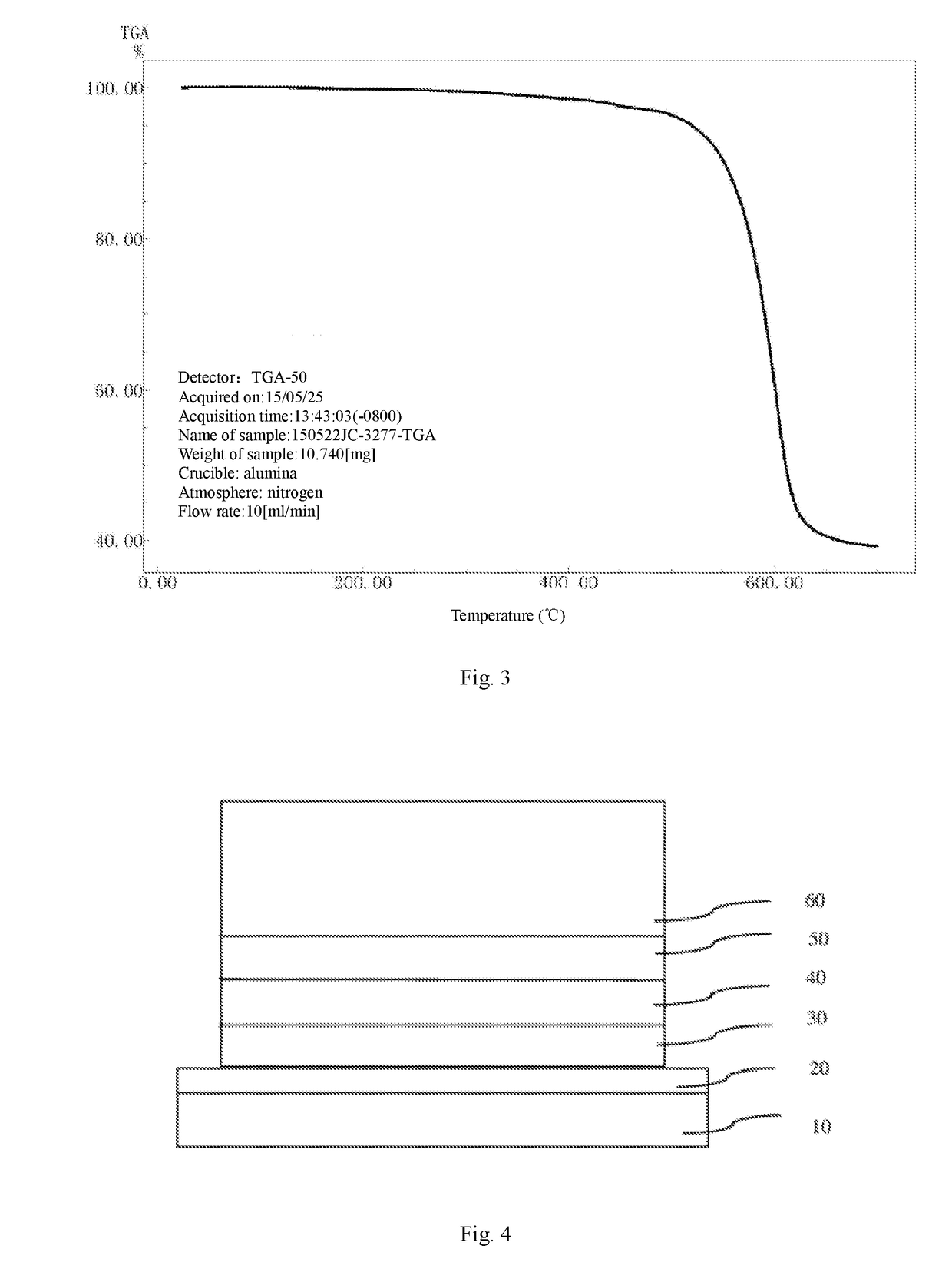
Synthesis of Compound 1
[0034]A compound A is synthesized according to the reference document: ACS Macro Letter, 2014, Processes 3, and 10-15. A compound B is synthesized according to the process of reference document: WO 2013182046 A1.
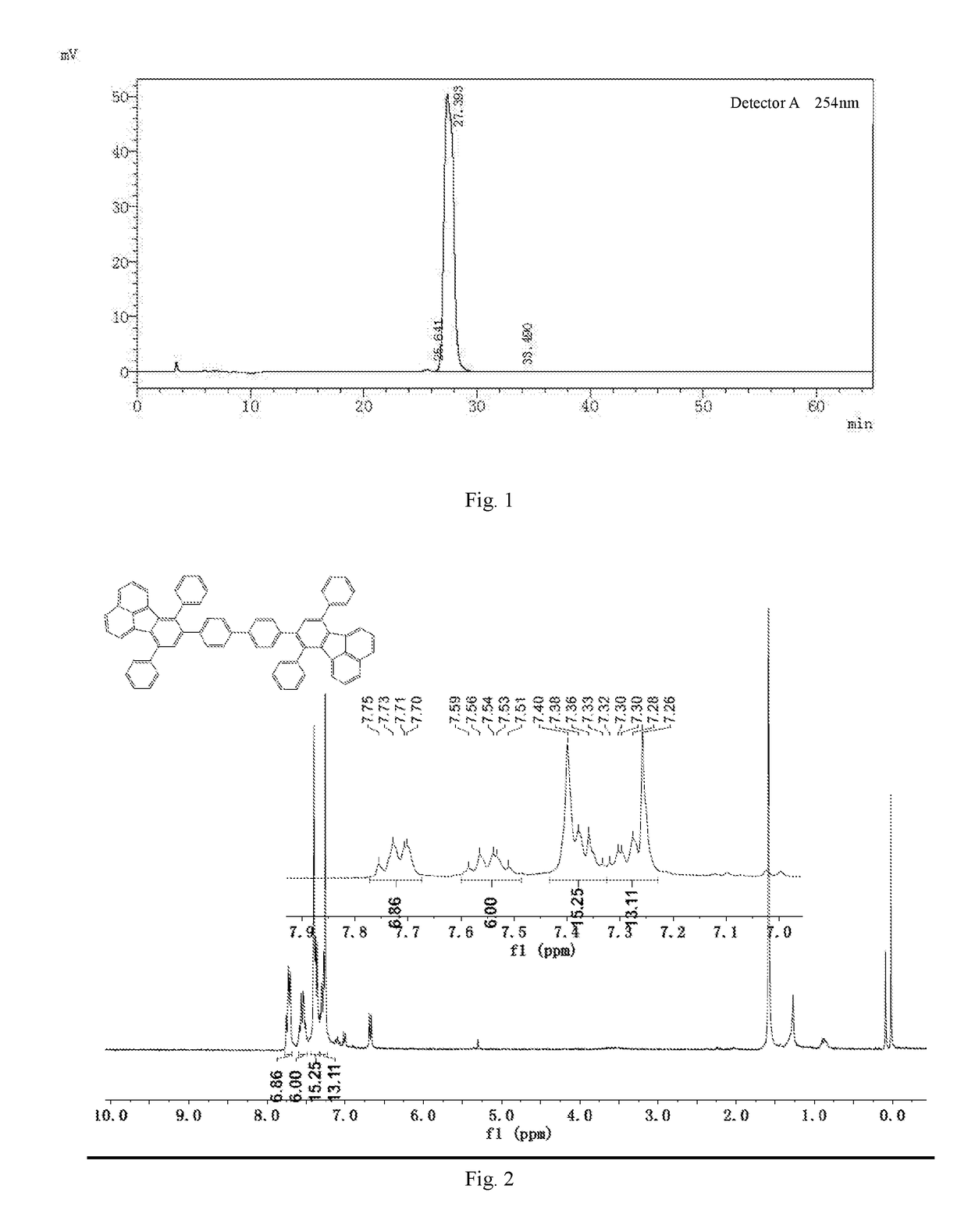
[0035]Reaction delivery: sequentially adding the compound A (2.21 g, 11 mmol), the compound B (7.80 g, 22 mmol), and diphenyl ether (100 mL) to a 250-mL reaction flask; after evacuating hydrogen three times, heating to 260° C., and preserving the heat and reacting for 8 hours till the compound B completely reacts under TLC and HPLC detection, the color of the reaction solution changing from black to yellow during the reaction.
[0036]Treatment after reaction: stopping heating and cooling to 20° C.; adding methanol (100 mL) and stirring for 2 h to separate solid out; washing a filter cake with methanol and drying in vacuum to obtain a crude product; adding ethyl acetate to the crude product and pulping to obtain a yellow compound 1 (4.32 g, yield 46...
example 2
Preparation of Electronic-Only Organic Semiconductor Diode Device 1
[0042]The electronic-only organic semiconductor diode device is manufactured by an organic electron transport material of the present invention.
[0043]First, a transparent conductive ITO glass substrate 10 (with an anode 20 on the top) is sequentially washed with a detergent solution and deionized water, ethanol, acetone and deionized water, and then subject to oxygen plasma treatment for 30 seconds.
[0044]Then, BCP which is 5 nm thick is evaporated on ITO as a hole barrier layer 30.
[0045]Then, a compound 1 which is 100 nm thick is evaporated on the hole injection layer as an electron transport layer 40.
[0046]Then, lithium fluoride which is 1 nm thick is evaporated on the electron transport layer as an electron injection layer 50.
[0047]At last, aluminum which is 100 nm thick is evaporated on the electron injection layer as a device cathode 60.
[0048]The structural diagram is as shown in FIG. 4.
[0049]By using the space c...
example 3
Preparation of Organic Electroluminescent Device 3
[0056]OLED is manufactured by the organic electronic material of the present invention.
[0057]First, a transparent conductive ITO glass substrate 10 (with an anode 20 on the top) is sequentially washed with a detergent solution and deionized water, ethanol, acetone and deionized water, and then subject to oxygen plasma treatment for 30 seconds.
[0058]Then, a compound C which is 90 nm thick is evaporated on ITO as a hole injection layer 30.
[0059]Then, a compound D is evaporated to form a hole transport layer 40 which is 30 nm thick.
[0060]Then, a compound E (2%) and a compound F (98%) which are 40 nm thick are evaporated on the hole transport layer as a light emitting layer 50.
[0061]Then, the compound 1 (50%) and LiQ (50%) which are 40 nm thick are evaporated on the light emitting layer as an electron transport layer 60.
[0062]At last, Al which is 100 nm thick is taken as a device cathode 70.
[0063](The structure diagram is as shown in FIG...
PUM
| Property | Measurement | Unit |
|---|---|---|
| Length | aaaaa | aaaaa |
| Angle | aaaaa | aaaaa |
| Angle | aaaaa | aaaaa |
Abstract
Description
Claims
Application Information