

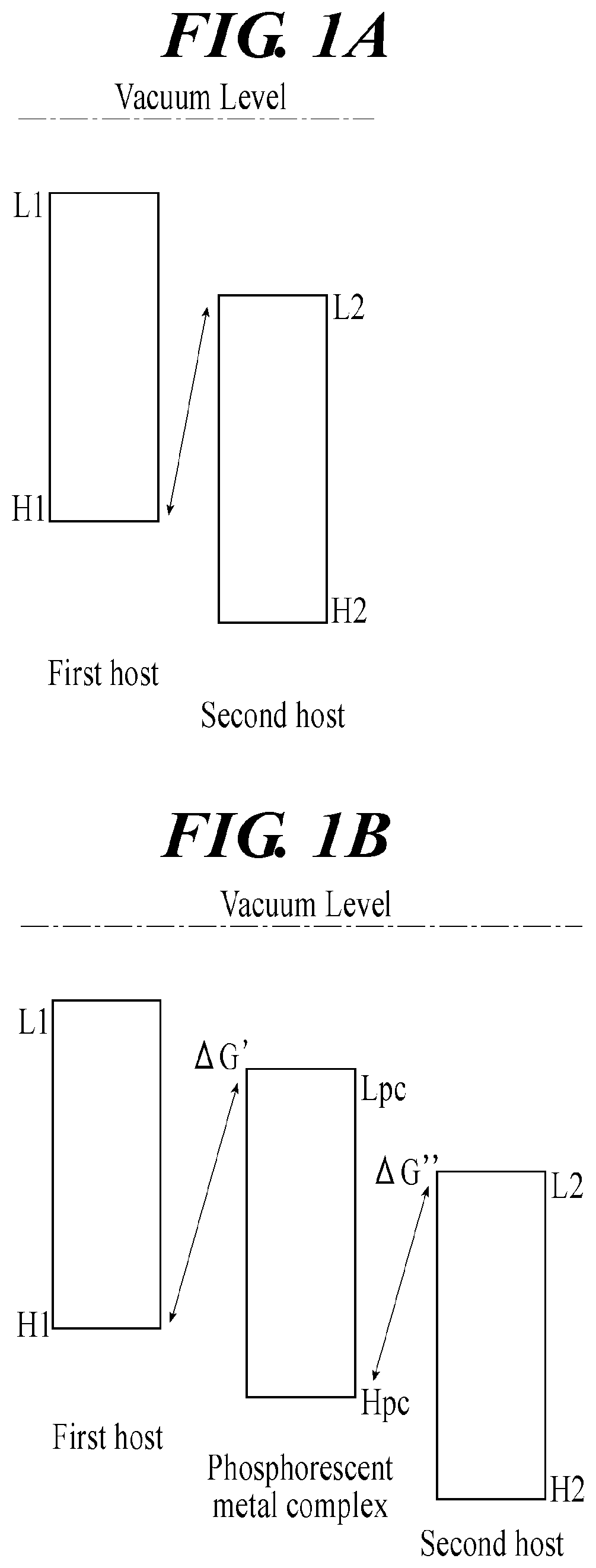
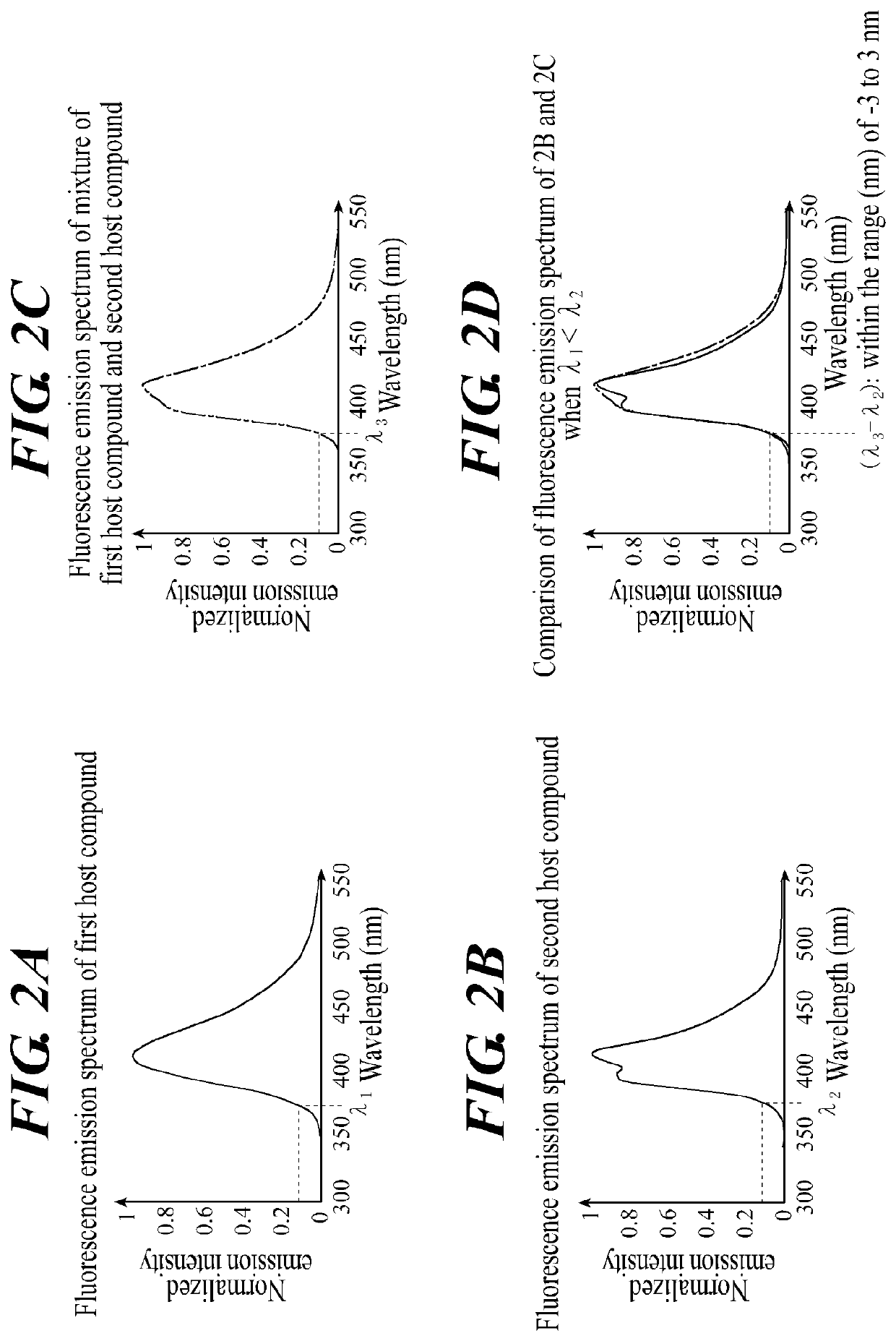
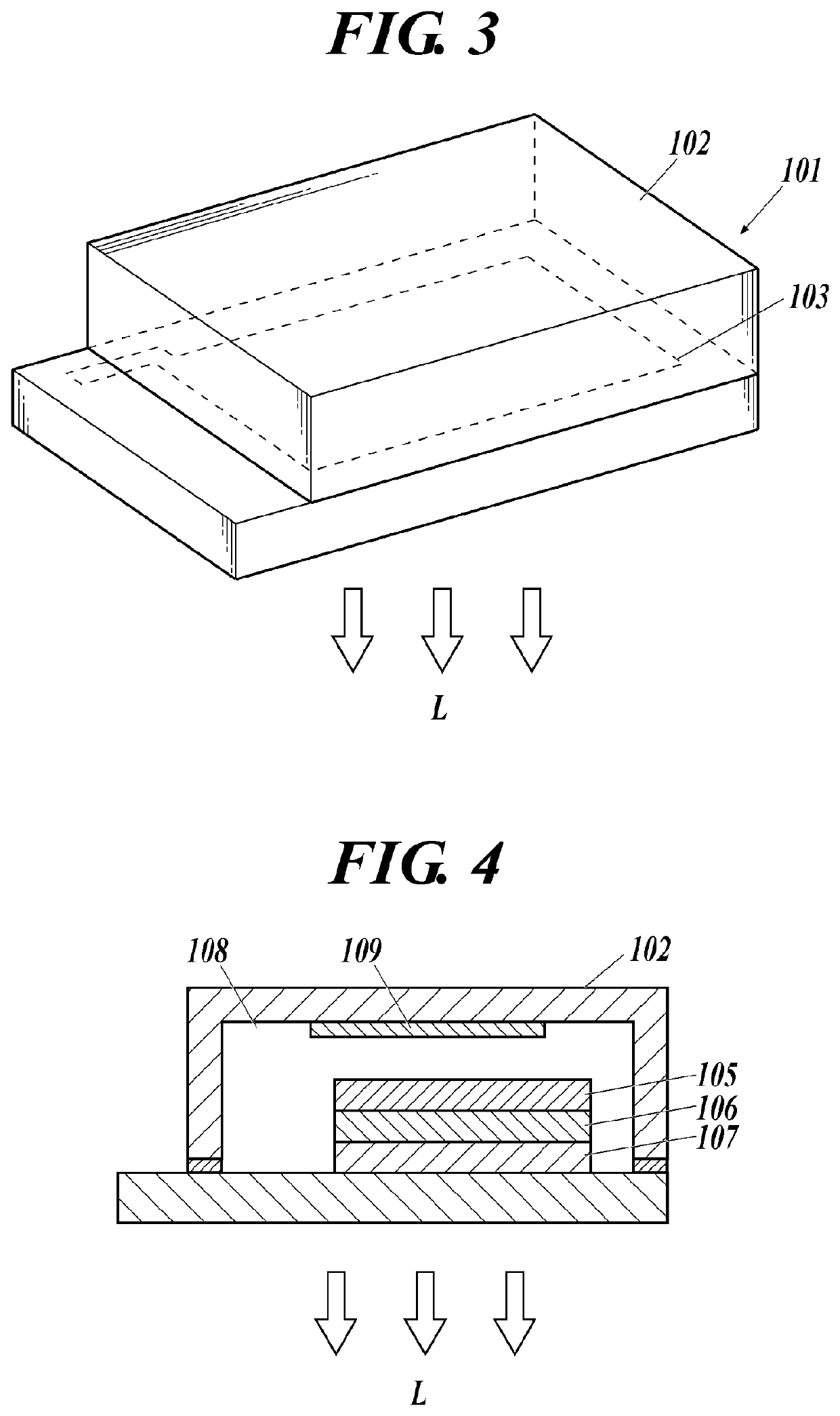
Organic electroluminescence element
a technology of electroluminescent elements and organic materials, applied in the direction of basic electric elements, electrical equipment, semiconductor devices, etc., can solve the problems of increasing power generation costs, affecting the efficiency of electroluminescent elements, so as to improve external quantum efficiency and element lifetime, wide gap, and high energy
- Summary
- Abstract
- Description
- Claims
- Application Information
AI Technical Summary
Benefits of technology
Problems solved by technology
Method used
Image

Examples
example 1
[0305]In Example 1, the characteristics of the vapor deposition film formation white light lighting device (organic EL element) containing the first host compound and the second host compound were evaluated.
(Preparation of Lighting Device 1-1)
[0306]An anode was prepared by making patterning to a glass substrate having a thickness of 0.7 mm on which ITO (indium tin oxide) was formed with a thickness of 110 nm. Thereafter, the above transparent support substrate provided with the ITO transparent electrode was subjected to ultrasonic washing with isopropyl alcohol, followed by drying with desiccated nitrogen gas, and was subjected to UV ozone washing for 5 minutes.
[0307]On the transparent support substrate thus prepared was applied a 70% solution of poly (3,4-ethylenedioxythiphene)-polystyrene sulfonate (PEDOT / PSS, Baytron P AI4083, made by Bayer ΔG.) diluted with water by using a spin coating method at 3,000 rpm for 30 seconds to form a film, and then it was dried at 130° C. for one h...
example 3
[0332]Next, in Example 3, the characteristics of the blue light emitting lighting device (and element) produced by the wet process using a coating liquid were confirmed.
«Preparation of Lighting Device for Evaluation»
(Preparation of Substrate)
[0333]First, on the entire surface of a polyethylene naphthalate film (hereinafter abbreviated as PEN) (manufactured by Teijin DuPont Films Co. Ltd.) on which the anode is to be formed, an atmospheric pressure plasma discharge treatment using an apparatus having the structure described in JP-A No. 2004-68143 was carried out to form an inorganic gas barrier layer made of SiOx having a thickness of 500 nm. In this way, a flexible substrate having gas barrier properties of an oxygen permeability of 0.001 ml / (m2·24 h) or less and a water vapor permeability of 0.001 g / (m2·24 h) or less was prepared.
(Formation of Anode)
[0334]ITO (indium tin oxide) having a thickness of 120 nm was formed on the above-described substrate by a sputtering method and patte...
example 4
[0369]Next, in Example 4, the characteristics of a blue-emitting lighting device (organic EL element) produced by an ink-jet (hereinafter, abbreviated as IJ) process were confirmed.
<
(Preparation of Substrate)
[0370]First, on the entire surface of a polyethylene naphthalate film (hereinafter abbreviated as PEN) (manufactured by Teijin DuPont Films Co. Ltd.) on which the anode is to be formed, an atmospheric pressure plasma discharge treatment using an apparatus having the structure described in JP-A No. 2004-68143 was carried out to form an inorganic gas barrier layer made of SiOx having a thickness of 500 nm. In this way, a flexible substrate having gas barrier properties of an oxygen permeability of 0.001 mL / (m2·24 h) or less and a water vapor permeability of 0.001 g / (m2·24 h) or less was prepared.
(Formation of Anode)
[0371]ITO (indium tin oxide) having a thickness of 120 nm was formed on the above-described substrate by a sputtering met...
PUM
| Property | Measurement | Unit |
|---|---|---|
| excited triplet energy level | aaaaa | aaaaa |
| temperature | aaaaa | aaaaa |
| fluorescence emission | aaaaa | aaaaa |
Abstract
Description
Claims
Application Information