

High speed / low power server farms and server networks
a server farm and low power technology, applied in the direction of process and machine control, instrument details, semiconductor/solid-state device details, etc., can solve the problems of consuming mega-watts of electrical power, affecting the operation of server farms, so as to reduce proximity losses and flux jumping losses, reduce magnetic saturation, and reduce spurious noise.
- Summary
- Abstract
- Description
- Claims
- Application Information
AI Technical Summary
Benefits of technology
Problems solved by technology
Method used
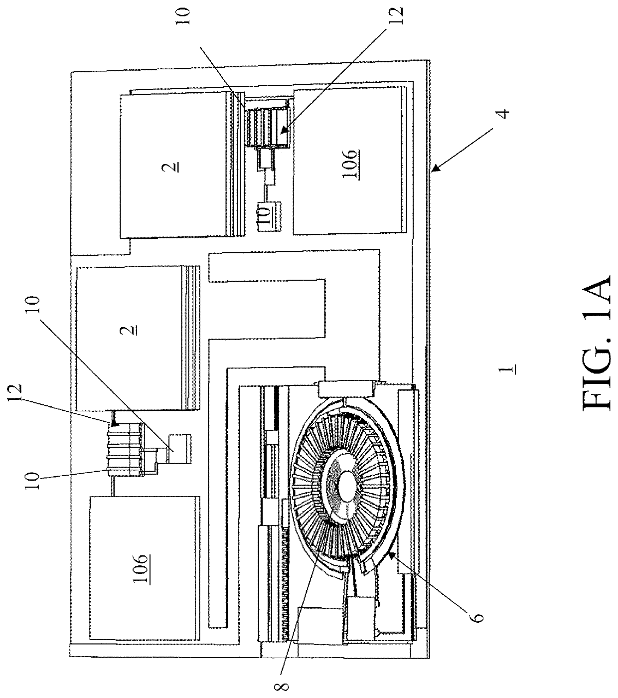
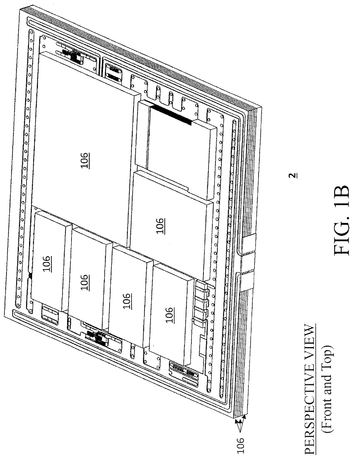
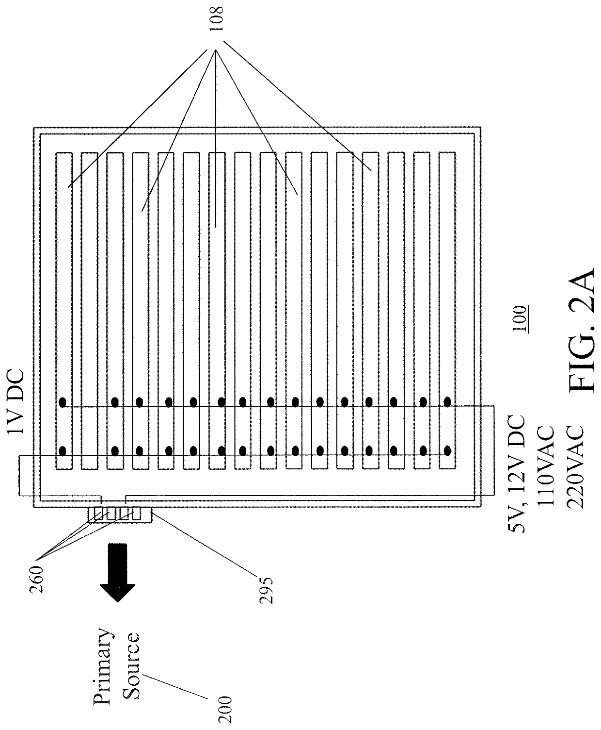
Image

Examples
Embodiment Construction
[0073]The present invention is illustratively described above in reference to the disclosed embodiments. Various modifications and changes may be made to the disclosed embodiments by persons skilled in the art without departing from the scope of the present invention as defined in the appended claims.
[0074]This application incorporates by reference all matter contained in de Rochemont U.S. Pat. No. 7,405,698 entitled “CERAMIC ANTENNA MODULE AND METHODS OF MANUFACTURE THEREOF” (the '698 application), de Rochemont U.S. Pat. No. 8,715,839 filed Jun. 30, 2006, entitled “ELECTRICAL COMPONENT AND METHOD OF MANUFACTURE” (the '839 application), de Rochemont U.S. Pat. No. 8,350,657 (the '657 application), filed Jan. 6, 2007 entitled “POWER MANAGEMENT MODULE AND METHODS OF MANUFACTURE”, de Rochemont U.S. Ser. No. 14 / 560,935, (the '935 application), filed Dec. 4, 2014 entitled “POWER MANAGEMENT MODULE AND METHODS OF MANUFACTURE”, de Rochemont, U.S. Ser. No. 13 / 216,192, “POWER FET WITH A RESONA...
PUM
| Property | Measurement | Unit |
|---|---|---|
| grain size distribution | aaaaa | aaaaa |
| grain size distribution | aaaaa | aaaaa |
| thickness | aaaaa | aaaaa |
Abstract
Description
Claims
Application Information