Check patentability & draft patents in minutes with Patsnap Eureka AI!

Active matrix substrate, microfluidic device including active matrix substrate, and method of manufacturing active matrix substrate and microfluidic device

Active Publication Date: 2020-10-01
SHARP KK
View PDF0 Cites 1 Cited by
  • Summary
  • Abstract
  • Description
  • Claims
  • Application Information

AI Technical Summary

Benefits of technology

The patent text discusses the use of a dielectric layer composed of a silicon nitride film formed by plasma chemical vapor deposition (plasma CVD) in electrowetting devices. The use of this dielectric layer reduces the actuation voltage required for the device, while a silicon oxide film improves adhesion on the fluorine resin but with a lower permittivity. The technical effect is to improve the performance of electrowetting devices by reducing operations voltage and improving adhesion.

Problems solved by technology

To use an SOG-based insulating film in an AM-EWOD device including TFTs, however, the calcination step where SOG is vitrified at about 300° C. can negatively affect the characteristics of the TFTs.
The silicon nitride film can however fail in some cases to deliver sufficient adhesion on the fluorine resin contained in the water-repelling layer, which would lead to the peeling of layers during manufacture and also to insufficient water-repelling properties and leak resistance.
Meanwhile, a silicon oxide (SiOx) film, if used in place of the silicon nitride film as a dielectric layer, improves adhesion on the fluorine resin, but leads to a low permittivity, thereby undesirably requiring an increased electrowetting actuation voltage.

Method used


Image

  • Active matrix substrate, microfluidic device including active matrix substrate, and method of manufacturing active matrix substrate and microfluidic device
  • Active matrix substrate, microfluidic device including active matrix substrate, and method of manufacturing active matrix substrate and microfluidic device
  • Active matrix substrate, microfluidic device including active matrix substrate, and method of manufacturing active matrix substrate and microfluidic device

Examples


embodiment 1

[0034]The present embodiment will describe, as an example of a microfluidic device in accordance with the present invention, an active matrix electrowetting-on-dielectric (AM-EWOD) device that uses thin film transistors (TFTs) to actuate a droplet (electrowetting-on-dielectric) in an active matrix array.

[0035]A description is now given of an embodiment of the present invention with reference to FIGS. 1 to 5.

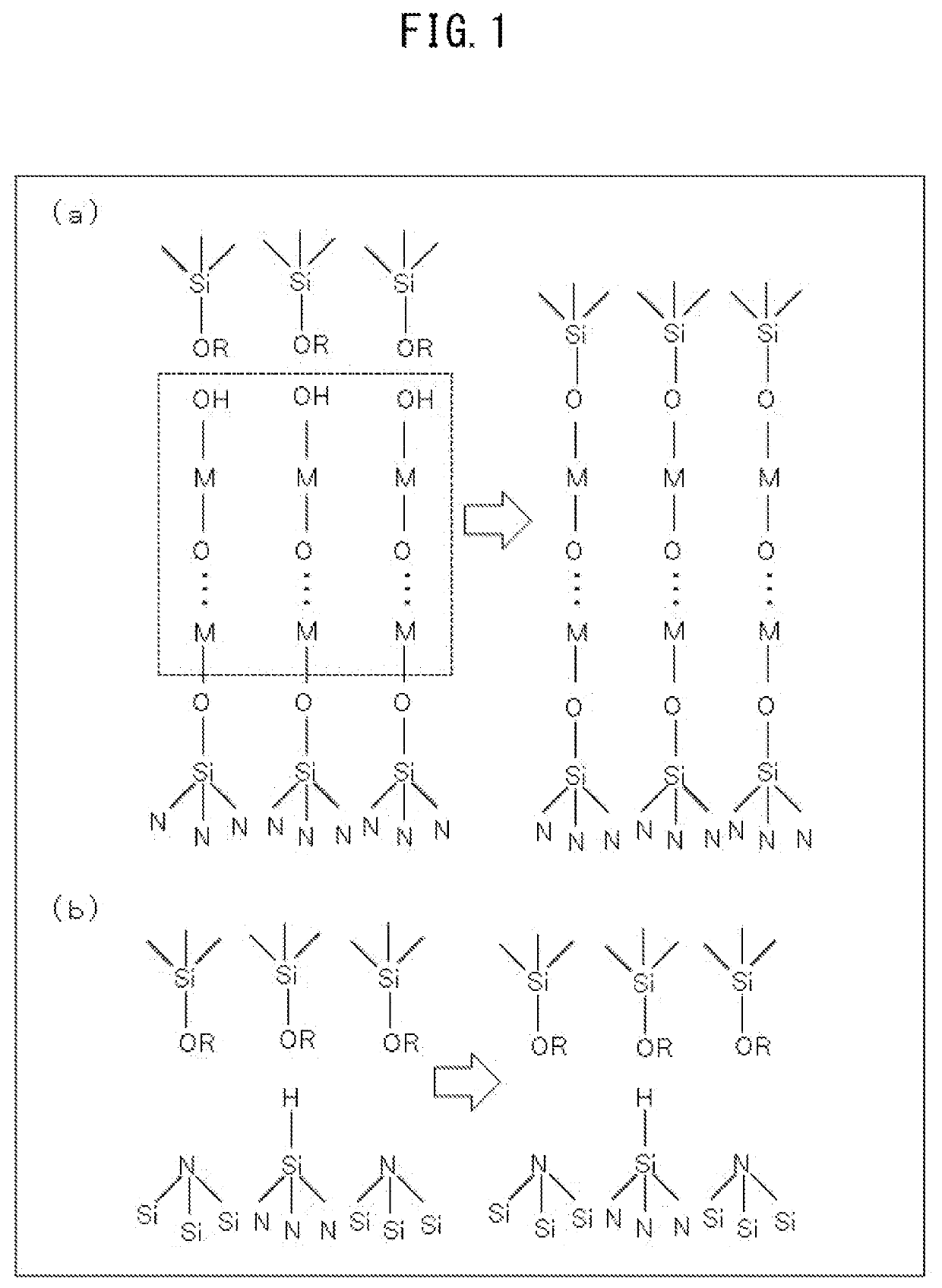
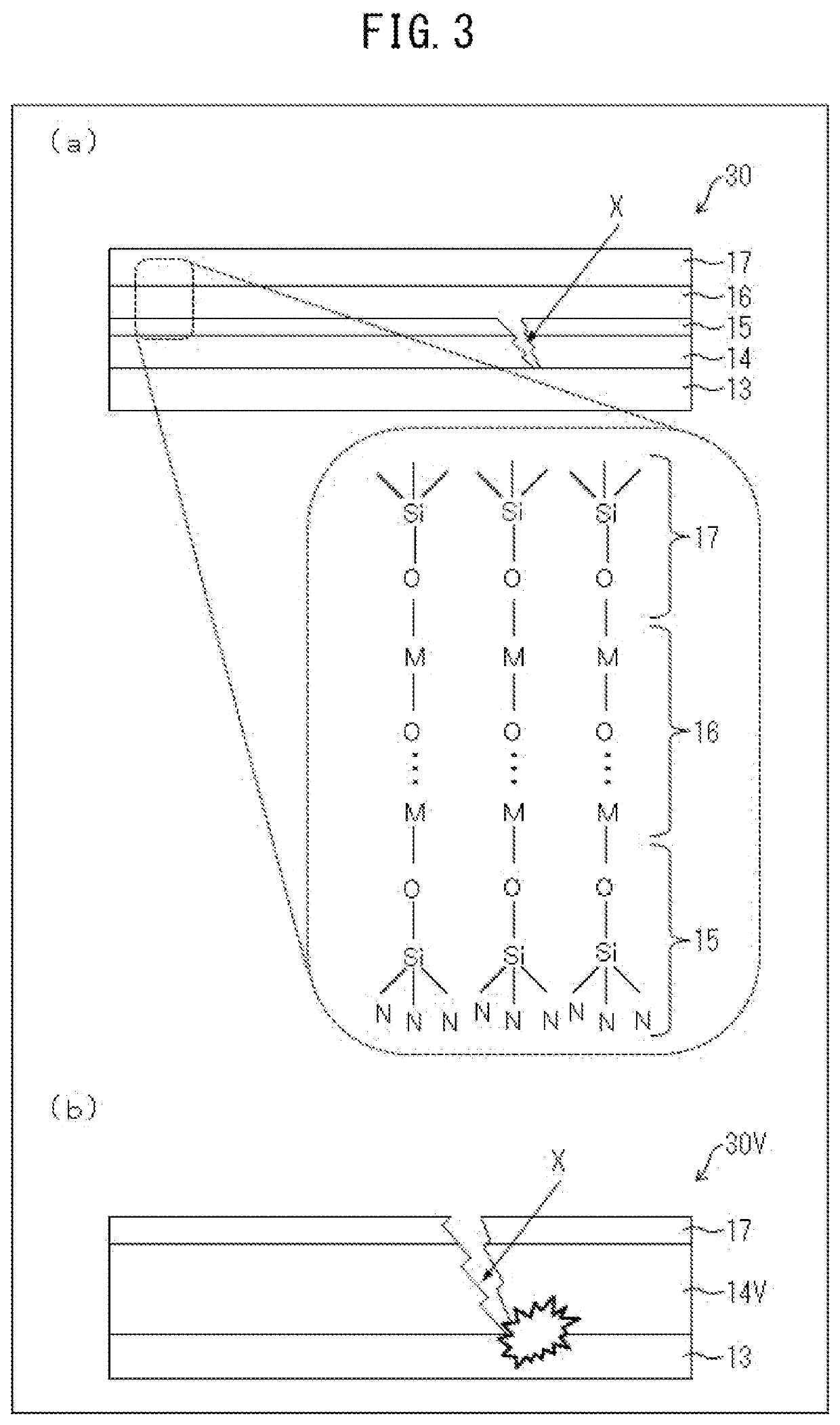
[0036]Portion (a) of FIG. 1 is a schematic illustration of bonding of an oxidized silicon nitride film surface, a metal-oxide film, and a water-repelling layer surface. Portion (b) of FIG. 1 is a schematic illustration of the condition of a silicon nitride film surface and a water-repelling layer surface in a conventional active matrix substrate.

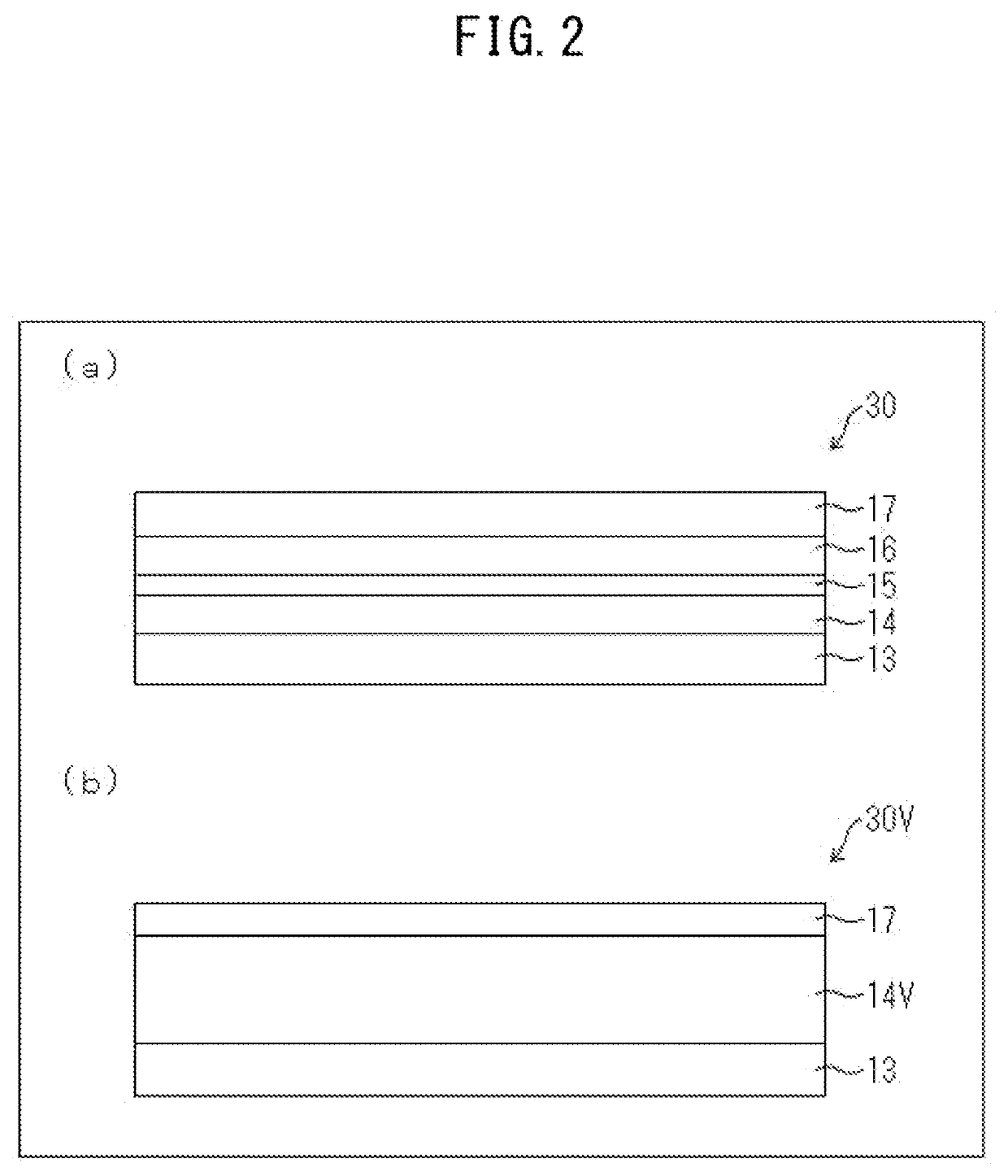
[0037]Portion (a) of FIG. 2 is a schematic cross-sectional view of an active matrix substrate accordance with Embodiment 1 of the present invention. Portion (b) of FIG. 2 is a schematic cross-sectional view of a conventional active matrix...

embodiment 2

[0079]A description is now given of another embodiment of the present invention with reference to FIGS. 6 and 7.

[0080]FIG. 6 is an illustration of a method of manufacturing an active matrix substrate in accordance with the present embodiment. FIG. 7 is an illustration of a method of manufacturing an opposite substrate in accordance with the present embodiment.

[0081]First, as shown in (a) of FIG. 6, a butler layer 101 is formed on a glass substrate (first substrate) 100. The buffer layer 101 may be, for example, a film of SiNx, Si)2, or SiNO with a thickness of approximately 100 to 300 nm. The buffer layer may have either a monolayer structure or a multilayer structure including a stack of two or more films and may also be omitted altogether in some devices. There is formed a semiconductor layer 102 on the buffer layer 101. The semiconductor layer 102 is a Si film with a thickness of approximately 20 to 100 nm and may be photo / dry-etched for patterning after being formed and crystall...

embodiment 3

[0101]A description is now given of another embodiment of the present invention.

[0102]The present embodiment differs from Embodiment 2 in that in the former, the metal-oxide film in the dielectric layer is formed by sputtering. The following describe another embodiment of present invention,

[0103]Similarly to the previous embodiment, a dielectric layer 111 is obtained by forming a silicon nitride (SiNx) film by plasma CVD, oxidizing the surface of the film to form a surface layer region having a high oxygen concentration, and forming a metal-oxide film on the surface layer region by DC sputtering. More specifically, a metal-oxide film is formed with a thickness of approximately 30 to 100 nm by using a sintered metal oxide as a target material, introducing argon and gaseous oxygen into a film-forming chamber, and heating the substrate to a temperature of 200° C. The metal-oxide film is formed at a rate of 10 nm / scan. A particularly preferred metal-oxide material is hafnium oxide (HFO2...


PUM


Abstract

An active matrix substrate includes: a first substrate; and first electrodes, a dielectric layer covering the first electrodes, and a first water-repelling layer in this sequence on the first substrate, wherein the dielectric layer has a multilayer structure including two or more layers and includes a silicon nitride film and a metal-oxide film between the silicon nitride film and the first water-repelling layer, and the silicon nitride film has an oxygen-containing surface layer region on a surface thereof that is in contact with the metal-oxide film.

Description

CROSS-REFERENCE TO RELATED APPLICATION[0001]The present application claims priority from Provisional Application No. 62 / 826,470, the content to which is hereby incorporated by reference into this application.BACKGROUND OF THE INVENTION1. Field of the Invention[0002]The present invention relates to active matrix substrates, microfluidic devices including an active matrix substrate, and methods of manufacturing active matrix substrates and microfluidic devices.2. Description of the Related Art[0003]Microfluidics and related technology requires manipulation and precise control of a tiny amount of fluid (ex., in submicroliters). Electrowetting (EW), capable of manipulating droplets by applying an electric field, is accordingly receiving increasing attention to fill these needs.[0004]Electrowetting is a phenomenon where under an applied voltage, a droplet placed on a water-repelling layer that is in turn on a dielectric layer covering an electrode changes its contact angle to the surface...

Claims


Application Information

Patent Timeline
IPC IPC(8): H01L27/12H01L29/786G02B26/00
CPCH01L27/1248H01L27/1244H01L29/7869G02B26/005H01L27/1225H01L27/1259G02B2207/115
Inventor HACHIYA, ATSUSHIFURUKAWA, HIROAKITSUJINO, KAZUYA
Owner SHARP KK
Features
  • R&D
  • Intellectual Property
  • Life Sciences
  • Materials
  • Tech Scout
  • Unparalleled Data Quality
  • Higher Quality Content
  • 60% Fewer Hallucinations
Learn More