Silicon-based lithium niobate film electro-optic modulator array and integration method thereof

Active Publication Date: 2020-11-19
SHANGHAI JIAO TONG UNIV
View PDF0 Cites 3 Cited by
  • Summary
  • Abstract
  • Description
  • Claims
  • Application Information

AI Technical Summary

Benefits of technology

[0026]Compared with the current technology, the silicon-based lithium niobate film electro-optic modulator array and the integration method thereof provided by the invention have the following advantages:
[0027]1. Complex structures such as modulator interconnection, optical splitters, breakpoints and optical couplers are realized in the silicon waveguide layers, and functional effectiveness and stability of the large-scale silicon-based lithium niobate film electro-optic modulator array are guaranteed.
[0028]2. By virtue of the design of the periodic structure, the large-scale silicon-based lithium niobate film electro-optic modulator array can be fabricated simultaneously at one time, besides, the lithium niobate film layer does not need to be cut, and the difficulty of bonding the modulator array is a

Problems solved by technology

However, the use of the doped silicon as a light guiding medium brings several problems as follows: doped silicon can absorb light, which may obviously increase the insertion loss of the electro-optic modulators; and the modulation efficiency of the doped silicon is low, so that the half-wave voltage

Method used


Image

  • Silicon-based lithium niobate film electro-optic modulator array and integration method thereof
  • Silicon-based lithium niobate film electro-optic modulator array and integration method thereof
  • Silicon-based lithium niobate film electro-optic modulator array and integration method thereof

Examples


Embodiment Construction

[0035]The technical scheme of the invention is described below in detail with reference to the accompanying drawings and the embodiments, and detailed implementations and structures are provided, but the protection scope of the invention is not limited to the following embodiments.

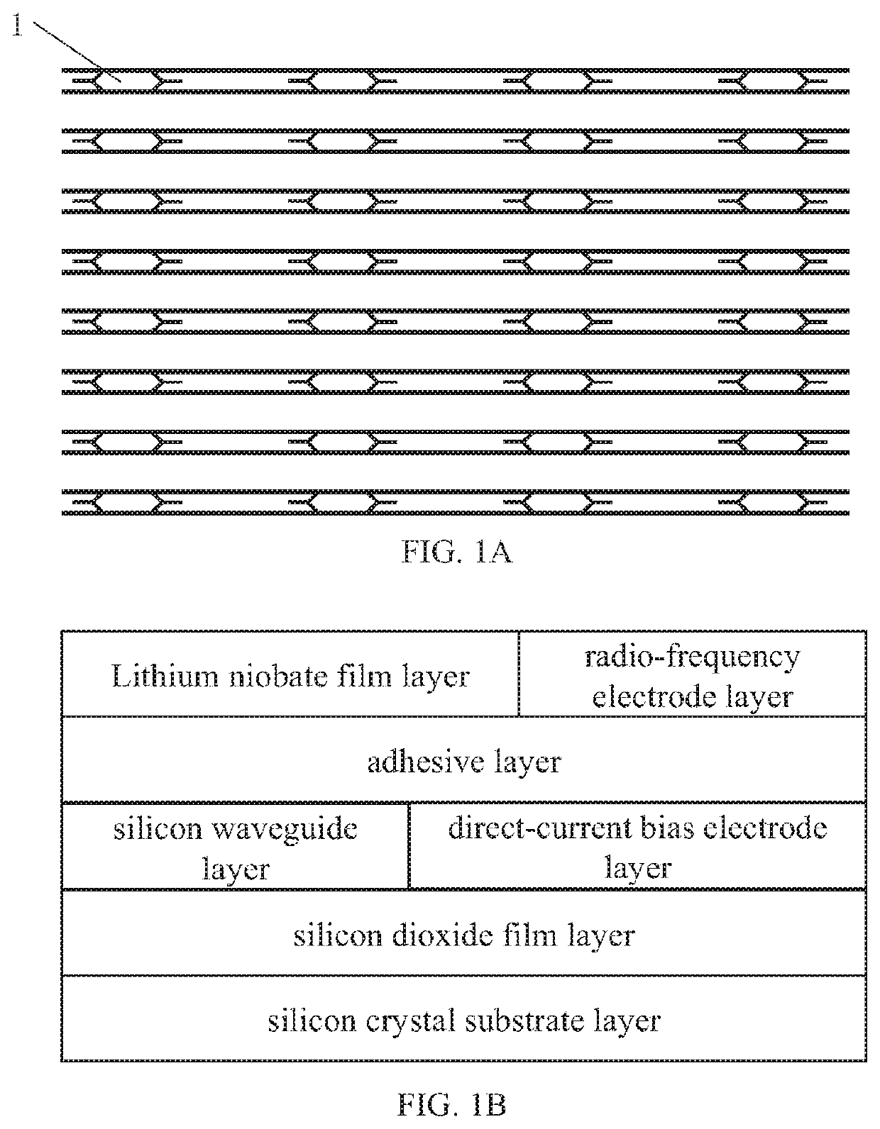
[0036]Referring to FIGS. 1A to 1D, which show partial structure schematic diagram of a silicon-based lithium niobate film electro-optic modulator array according to the embodiment of the present invention, an integration method of the silicon-based lithium niobate film electro-optic modulator array according to the present invention comprises the following steps that:

[0037](1) a smooth silicon crystal substrate 2 is oxidized by thermal oxidation to form a silicon dioxide film layer 3;

[0038](2) polycrystalline silicon with a certain thickness is deposited on the silicon dioxide film layer 3 by chemical vapor deposition (CVD), and silicon waveguide layers 4 with a plurality of silicon-based lithium niobate f...


PUM


Abstract

Integration method of a large-scale silicon-based lithium niobate film electro-optic modulator array. By using the method, the difficulty of a fabrication process of a lithium niobate crystal layer is reduced, requirements on precision of bonding lithium niobate and silicon is reduced, and fabrication and bonding of the large-scale array lithium niobate crystal layer can be completed at one time, so that production efficiency of the silicon-based lithium niobate film electro-optic modulator array is greatly improved; through design and optimization of the structure of the silicon crystal layers, light can be naturally alternated and mutually transmitted in silicon waveguides and lithium niobate waveguides, and a high-performance electro-optic modulation effect of the lithium niobate film is achieved.

Description

CROSS-REFERENCE TO RELATED APPLICATION[0001]The subject application claims priority on Chinese patent application nos. 201910410940.0 and 201910410956.1, both filed on May 17, 2019 in China. The contents and subject matter of the Chinese priority applications are incorporated herein by reference.TECHNICAL FIELD[0002]The present invention relates to optoelectronic integrated devices, in particular to a silicon-based lithium niobate film electro-optic modulator array and an integration method thereof.BACKGROUND ART[0003]Electro-optic modulators load electrical signals onto optical signals and serve as signal input interfaces of optical signal processing systems for optical communication, microwave photon radar, and the like. The performance of the optical signal processing systems directly depends on the performance of the electro-optic modulators, making the electro-optic modulators important photonic devices. In order to integrate the electro-optic modulators on a chip, the electro-...

Claims


Application Information

Patent Timeline
IPC IPC(8): G02F1/225G02F1/035G02B6/42
CPCG02B2006/12038G02B6/4279G02B2006/12061G02F1/225G02B2006/1204G02F1/035G02F2001/217G02B2006/12059G02B2006/12107G02B2006/12147G02B2006/1215G02F1/217G02B2006/12176G02B2006/12188G02F1/015
Inventor ZOU, WEIWENXU, SHAOFUWANG, JINGCHEN, JIANPING
Owner SHANGHAI JIAO TONG UNIV
Why Eureka
Try Eureka