

Metal oxide-based chemical sensors
- Summary
- Abstract
- Description
- Claims
- Application Information
AI Technical Summary
Benefits of technology
Problems solved by technology
Method used
Image

Examples
example 1
[0136]A general description of the novel manufacturing process for making sensors and the highly-integrated sensors of the present invention is as follows:
[0137]Starting Substrate:
[0138]An oxidized silicon wafer is used as the substrate for the sensors and platforms of the present invention. A platform of the present invention is a unit that comprises multiple sensors and pairs of electrical leads and at least one heating element. The present manufacturing process allows for numerous platforms to be formed simultaneously on one oxidized silicon wafer. As will be described below, each platform may contain only one type of sensor (e.g., all sensors have the same metal oxide / dopant layers) or each sensor on the platform may have a variety of different sensor types (e.g., 2, 3, 4, or more).
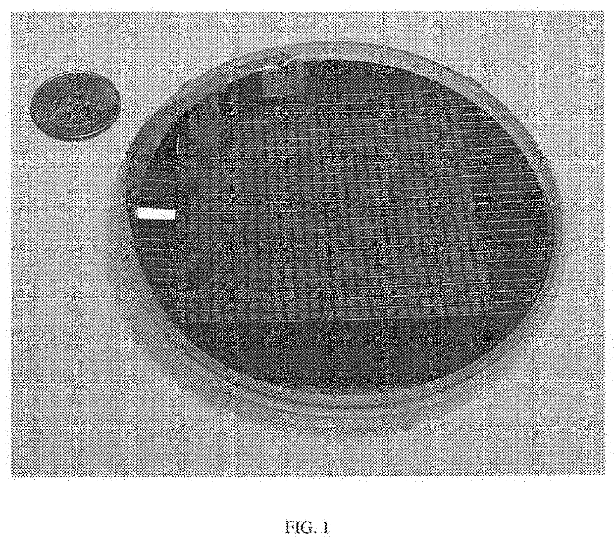
[0139]A typical wafer is 4″ in diameter, but a larger wafer (e.g., 6″ in diameter) can be used in order to increase the number of devices per manufacturing cycle and decrease the manufacturing cost pe...
example 2
[0206]H2S sensor
[0207]Step 1: Starting Substrate
[0208]A 4″ diameter oxidized silicon (100) wafer (200 μm with a 300 nm SiO2 top (polished) and bottom layers) was prepared by washing with deionized water (DI water) and then inspected under an optical microscope.
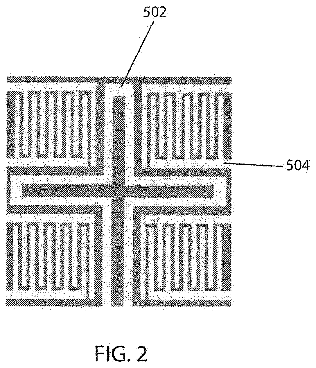
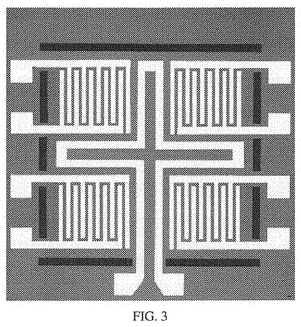
[0209]Step 2: Top Side Photolithography (Photomask #1)
[0210]To provide patterns for the heater and terminals, a photomask (photomask #1) was applied to the wafer using photolithography. Photoresist 1827 (a positive photoresist) was applied to the polished side of the wafer. The wafer was spun (Laurel EDC-650-23B Spin Processor) for 0.2 sec@ 500 rpm while the photoresist was applied, and then for 10 sec @ 4000 rpm.
[0211]After spin coating, the wafer was “soft baked” by heating at 90° C. in air for about 70-75 sec. The “soft baked” wafer was then exposed to UV light 325W for about 22 seconds, followed by a toluene bath (60 sec), blow drying with N2, and another soft baking (this time 90° C. for about 15 sec).
[0212]The photoresis...
example 3
[0267]Integrated Chemical Sensor:
[0268]An integrated chemical sensor (ICS) can be assembled using the platform packaged into a transistor outline as its sensor. The integrated sensor, further comprises: (a) a resistor network, comprising: a load resistor electrically connected to the sensors of the packaged sensor platform; and, (b)a logic element (e.g., transistor or a computer) electrically connected to the resistor.
[0269]Alternatively, in addition to the platform packaged into a transistor outline as its sensor, the ICS further comprises: (a) a resistor network, comprising: a load resistor electrically connected to the sensors of the packaged sensor platform; and, (b) an analog-to-digital converter (ADC), the ADC being electrically connected to the resistor network (e.g., can be attached to an explorer board); (c) a logic element (e.g., transistor or a computer) electrically connected to the ADC (e.g., electrically connected to the explorer board, if present); and, (d) optionally...
PUM
 Abstract
Description
Claims
Application Information