Epitaxial structure of gan-based radio frequency device based on si substrate and its manufacturing method

a radio frequency device and gan-based technology, applied in the field of epitaxial structure its manufacturing method, can solve the problems of poor material uniformity, high cost, and the only use of gan-based microwave power based on sic substrates in the military field, and achieve the effects of suppressing material failure, improving film quality, and high crystal quality

Active Publication Date: 2021-08-26
ZHONGSHAN INST OF MODERN IND TECH SOUTH CHINA UNIV OF TECH +1
View PDF1 Cites 2 Cited by
  • Summary
  • Abstract
  • Description
  • Claims
  • Application Information

AI Technical Summary

Benefits of technology

[0029]Compared with the prior art, the present invention has following advantages and technical effects:
[0030]The epitaxy is the epitaxial structure of the GaN-based radio frequency device based on the Si substrate. By optimizing the process conditions, on the one hand, the material failure is suppressed, and on the other hand, the film quality is improved. The epitaxy prepared on the large-sized Si substrate has characteristics of high crystal quality, good confinement of the channel carrier, low leakage current. The device prepared by the epitaxial structure of the present invention has high breakdown voltage, high current density, low off-state leakage, and excellent pinch-off characteristics, and has small performance degradation at high temperature. The epitaxial structure of the GaN-based radio frequency device based on the Si substrate has a simple manufacturing process and good repeatability, and is suitable for high-frequency, high-power wireless communication, radar and other applications.

Problems solved by technology

The main constraint of SiC substrate materials is the high cost, which leads to that the GaN-based microwave power based on SiC substrates can only be used currently in military fields such as active phased array radar, satellite and so on.
At present, the main difficulty in growing flat GaN-based epitaxial materials on the large-size Si substrates is that due to the huge lattice mismatch (−17%) and thermal mismatch (116%) between GaN and Si substrates, resulting in high wafer warpage, poor material uniformity and poor GaN crystal quality, so the defect density (including dislocations and background impurities) is high, and then the current leakage of the material is high, causing reliability problems of the device.

Method used


Image

  • Epitaxial structure of gan-based radio frequency device based on si substrate and its manufacturing method
  • Epitaxial structure of gan-based radio frequency device based on si substrate and its manufacturing method
  • Epitaxial structure of gan-based radio frequency device based on si substrate and its manufacturing method

Examples


embodiment 1

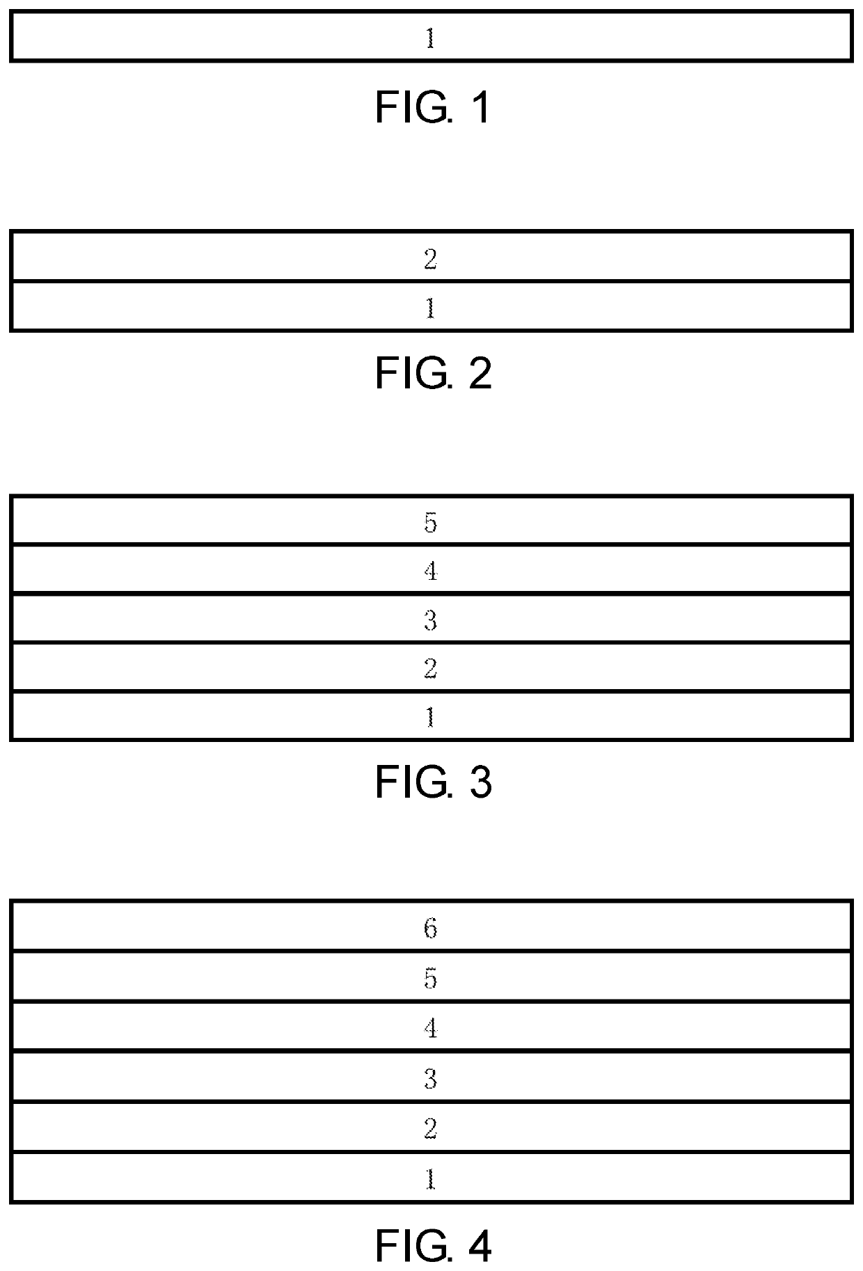
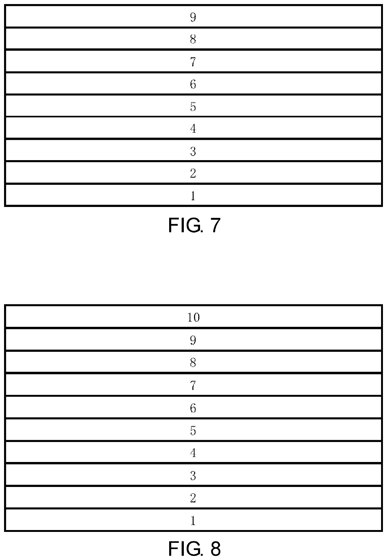
[0039]The Si substrate 1 has a circular shape and a diameter of 8 inches. The thicknesses of the Si substrate, the AlN nucleation layer, the GaN channel layer, the AlGaN barrier layer, and the GaN cap layer are 1 mm, 0.5 μm, 300 nm, 20 nm, and 3 nm, respectively.

[0040]The first AlGaN buffer layer 3, the second AlGaN buffer layer 4 and the third AlGaN buffer layer 5 have a total of three layers, wherein an Al element molar content of each of the three layers from bottom to top decreases in turn, which is 0.7, 0.5 and 0.3 respectively; the thickness of each of the three layers increases in turn, which is 300 nm, 500 nm and 700 nm respectively.

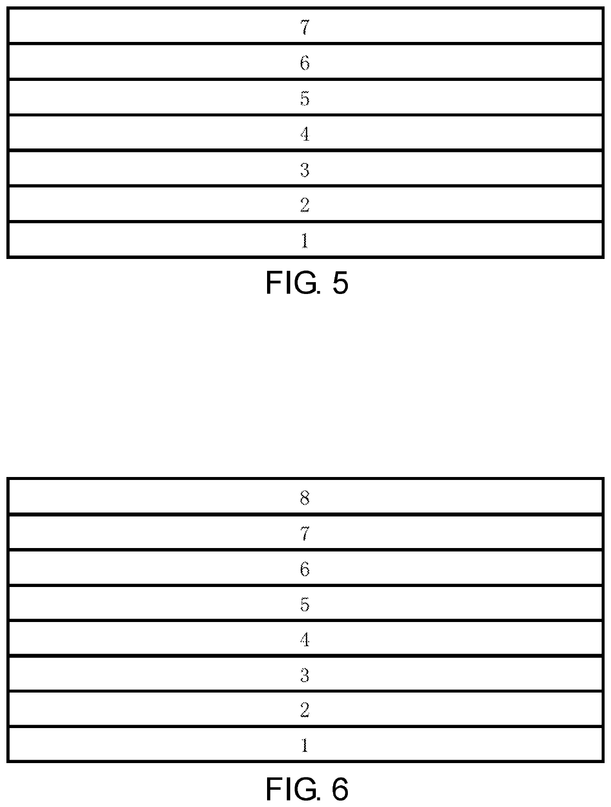
[0041]The GaN:Fe / GaN high-resistance layer 6 is composed of the intentional Fe-doped GaN layer and the unintentional doped GaN layer which are alternately connected. Each of the intentional Fe-doped GaN layer and the unintentional doped GaN layer has a thickness of 100 nm and a period of 3 cycles, and a doping concentration of Fe impurities in th...

embodiment 2

[0057]The Si substrate 1 has a circular shape and a diameter of 8 inches. The thicknesses of the Si substrate, the MN nucleation layer, the GaN channel layer, the AlGaN barrier layer, and the GaN cap layer are 1 mm, 0.5 μm, 300 nm, 30 nm, and 5 nm, respectively.

[0058]The first AlGaN buffer layer 3, the second AlGaN buffer layer 4 and the third AlGaN buffer layer 5 have a total of three layers, wherein an Al element molar content of each of the three layers from bottom to top decreases in turn, which is 0.7, 0.5 and 0.3 respectively; thickness of each of the three layers increases in turn, which is 300 nm, 500 nm and 700 nm respectively.

[0059]The GaN:Fe / GaN high-resistance layer 6 is composed of the intentional Fe-doped GaN layer and the unintentional doped GaN layer which are alternately connected. Each of the intentional Fe-doped GaN layer and the unintentional doped GaN layer has a thickness of 150 nm and a period of 5 cycles, and a doping concentration of Fe impurities in the int...

embodiment 3

[0075]The Si substrate 1 has a circular shape and a diameter of 8 inches. The thicknesses of the Si substrate, the MN nucleation layer, the GaN channel layer, the AlGaN barrier layer, and the GaN cap layer are 1 mm, 0.5 μm, 300 nm, 15 nm, and 2 nm, respectively.

[0076]The AlGaN buffer layers 3-5 have a total of three layers, wherein an Al element molar content of each of the three layers from bottom to top decreases in turn, which is 0.7, 0.5 and 0.3 respectively; thickness of each of the three layers increases in turn, which is 300 nm, 500 nm and 700 nm respectively.

[0077]The GaN:Fe / GaN high-resistance layer 6 is composed of the intentional Fe-doped GaN layer and the unintentional doped GaN layer which are alternately connected. Each of the intentional Fe-doped GaN layer and the unintentional doped GaN layer has a thickness of 100 nm and a period of 3 cycles, and a doping concentration of Fe impurities in the intentional Fe-doped GaN layer is 1E19 cm−3.

[0078]The GaN superlattice lay...


PUM

PropertyMeasurementUnit
thicknessaaaaaaaaaa
thicknessaaaaaaaaaa
thicknessaaaaaaaaaa

Abstract

An epitaxial structure of a GaN-based radio frequency device based on a Si substrate and a manufacturing method thereof are provided. The epitaxial structure is composed of a Si substrate (1), an AlN nucleation layer (2), AlGaN buffer layers (3, 4, 5), a GaN:Fe/GaN high-resistance layer (6), a GaN superlattice layer (7), a GaN channel layer (8), an AlGaN barrier layer (9) and a GaN cap layer (10) which are stacked in turn from bottom to top, wherein the GaN:Fe/GaN high-resistance layer (6) is composed of an intentional Fe-doped GaN layer and an unintentional doped GaN layer which are alternately connected; the GaN superlattice layer (7) is composed of a low-pressure/low V/III ratio GaN layer and a high-pressure/high V/III ratio GaN layer which are periodically and alternately connected.

Description

BACKGROUNDTechnical Field[0001]The present invention relates to semiconductor devices, in particular to an epitaxial structure of a GaN-based radio frequency device based on a Si substrate and its manufacturing method. The epitaxial structure of the GaN-based radio frequency device may be used in fields such as high-frequency, high-power wireless communication, radar and so on.Description of Related Art[0002]With the development of modern weaponry and aerospace, nuclear power, communication technology, automotive electronics, and switching power supplies, higher requirements are placed on the performance of semiconductor devices. As a typical representative of wide-bandgap semiconductor materials, GaN-based material has the characteristics such large width of bandgap, high electron saturation drift velocity, high critical breakdown field strength, high thermal conductivity, good stability, corrosion resistance, radiation resistance and so on, and may be used for manufacturing high-t...

Claims


Application Information

Patent Timeline
Patent Type & Authority Applications(United States)
IPC IPC(8): H01L29/778H01L29/205H01L29/20H01L29/207H01L21/02
CPCH01L29/7783H01L29/205H01L29/2003H01L29/207H01L21/0262H01L21/02458H01L21/02505H01L21/0254H01L21/0257H01L21/02381H01L29/0615H01L29/0634H01L29/66462H01L29/7786H01L21/02581H01L21/02507
Inventor WANG, HONGZHOU, QUANBIN
Owner ZHONGSHAN INST OF MODERN IND TECH SOUTH CHINA UNIV OF TECH
Why Eureka
Try Eureka