Composite substrate and method of manufacturing composite substrate

a technology of composite substrates and substrates, applied in the direction of impedence networks, electrical devices, etc., can solve the problems of increasing resistance of lt (or ln) layers, pyroelectric, and reducing the yield of device manufacturing processes, so as to suppress the increase in pyroelectricity caused by heat-treatment processes

Pending Publication Date: 2021-10-21
SHIN ETSU CHEM IND CO LTD
View PDF0 Cites 0 Cited by
  • Summary
  • Abstract
  • Description
  • Claims
  • Application Information

AI Technical Summary

Benefits of technology

[0010]By providing a diffusion prevention layer that prevents diffusion of oxygen between an LT layer (or LN layer) and a support substrate in a composite substrate, the increase in pyroelectricity is suppressed. The inventor found that the oxygen contained in the intervening layer or the support substrate diffuses into the LT layer (or LN layer) by heat treatment, which increases the resistivity of the LT layer (or LN layer) and makes it more pyroelectric. The present invention prevents excessive oxygen diffusion into the LT layer (or LN layer) of the composite substrate by providing a diffusion prevention layer between the LT layer (or LN layer) and the intervening layer, or by forming the intervening layer with a material that has a diffusion prevention effect. In this way, the increase in pyroelectricity of the LT layer (or LN layer) of the composite substrate is suppressed.
[0011]The composite substrate of an embodiment of the present invention has an oxide single crystal thin film, which is a single crystal thin film of a piezoelectric material, a support substrate, and a diffusion prevention layer that is provided between the oxide single crystal thin film and the support substrate to prevent the diffusion of oxygen.

Problems solved by technology

However, when surface acoustic wave devices are manufactured using composite substrate wafers with LT (or LN) bonded to a support substrate with enhanced conductivity in this way, the resistivity of the LT (or LN) layer may increase and become pyroelectric as it undergoes heat treatment in the wafer process and device process.
In addition, temperature changes during the process can cause charges to accumulate on the surface of the composite substrate.
If sparks occur, the pattern formed on the substrate surface is destroyed, resulting in lower yields in the device manufacturing process.

Method used


Image

  • Composite substrate and method of manufacturing composite substrate
  • Composite substrate and method of manufacturing composite substrate

Examples


example 1

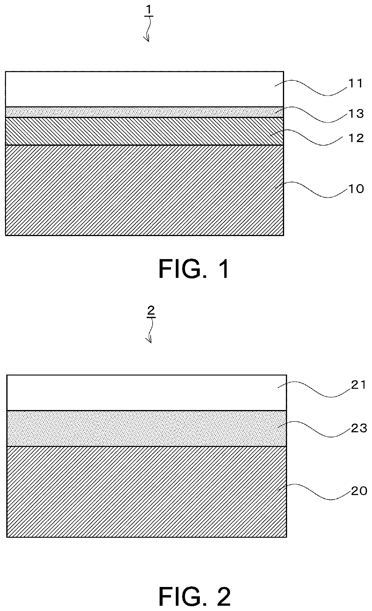
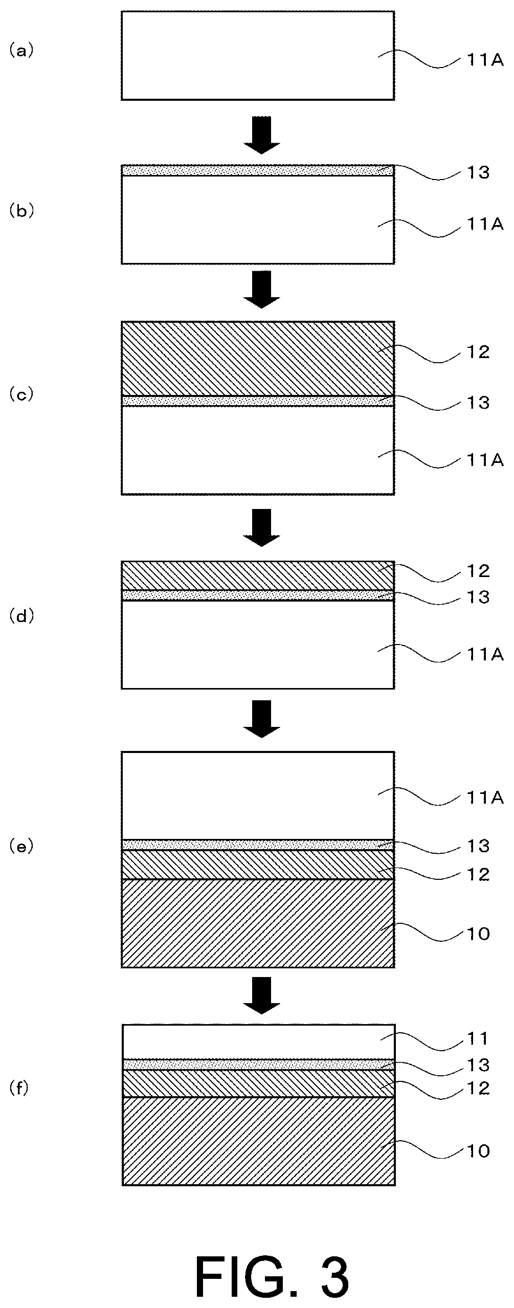
[0035]Approximately 25 nm of SiN was deposited on one side of an LT wafer with a diameter of 150 mm by the PVD method to form a diffusion prevention layer. Then, a silicon oxide film was formed on this diffusion prevention layer by CVD to a thickness of about 3 μm. The silicon oxide film was polished and bonded to a p-type silicon wafer with a resistivity of 2000 Ωcm using this silicon oxide film as an intervening layer. The LT wafers used are highly conductive, with bulk conductivity of about 4×10⁻¹¹ / Ωcm. After the bonding, heat treatment was applied in a nitrogen atmosphere at 100° C. for 48 hours. The LT layer was then thinned by grinding and polishing to a thickness of 20 μm. Then, to further increase the bonding strength, heat treatment was performed at 250° C. for 24 hours in a nitrogen atmosphere.

[0036]The pyroelectricity of the bonded substrate manufactured as described above was evaluated by surface potential. The bonded substrate was placed on a hot plate at 250° C. for 20...

example 2

[0039]Approximately 25 nm of SiN was deposited on one side of an LT wafer with a diameter of 150 mm by the PVD method to form a diffusion prevention layer. Then, a silicon oxide film was formed on this diffusion prevention layer by CVD to a thickness of about 3 μm. The silicon oxide film was polished and bonded to a p-type silicon wafer with a resistivity of 2000 Ωcm using this silicon oxide film as an intervening layer. Prior to the bonding, the bonding surface was surface activated by the plasma activation method. The LT wafers used are highly conductive, with bulk conductivity of about 4×10⁻¹¹ / Ωcm. After the bonding, heat treatment was applied in a nitrogen atmosphere at 100° C. for 48 hours. The LT layer was then thinned by grinding and polishing to a thickness of 20 μm. Then, to further increase the bonding strength, heat treatment was performed at 250° C. for 24 hours in a nitrogen atmosphere.

[0040]The pyroelectricity of the bonded substrate manufactured as described above was...

examples 3 , 4

Examples 3, 4

[0041]Approximately 25 nm of SiN diffusion prevention film was deposited on one side of an LT wafer with a diameter of 150 mm by the PVD method to form a diffusion prevention layer. Then, a silicon oxide film was formed on this diffusion prevention layer by CVD to a thickness of about 3 μm. The silicon oxide film was polished, and after surface activation, bonded to a p-type silicon wafer with a resistivity of 2000 Ωcm using this silicon oxide film as an intervening layer. Prior to the bonding, the bonding surface was surface activated by various activation methods (ion beam activation method, ozone water activation method). The LT wafers used are highly conductive, with bulk conductivity of about 4×10⁻¹¹ / Ωcm. After the bonding, heat treatment was applied in a nitrogen atmosphere at 100° C. for 48 hours. The LT layer was then thinned by grinding and polishing to a thickness of 20 μm. Then, to further increase the bonding strength, heat treatment was performed at 250° C....


PUM

PropertyMeasurementUnit
diameteraaaaaaaaaa
diameteraaaaaaaaaa
thicknessaaaaaaaaaa

Abstract

A composite substrate with suppressed pyroelectricity increase due to the heat-treatment process is provided. The composite substrate has an oxide single crystal thin film, which is a single crystal thin film of a piezoelectric material, a support substrate, and a diffusion prevention layer that is provided between the oxide single crystal thin film and the support substrate to prevent the diffusion of oxygen. The diffusion prevention layer may have any of silicon oxynitride, silicon nitride, silicon oxide, magnesium oxide, spinel, titanium nitride, tantalum, tantalum nitride, tungsten nitride, aluminum oxide, silicon carbide, tungsten boron nitride, titanium silicon nitride, and tungsten silicon nitride.

Description

TECHNICAL FIELD[0001]The present invention relates to a composite substrate for surface acoustic wave devices and a method for manufacturing the same.BACKGROUND ART[0002]In recent years, in the field of mobile communications typified by smartphones, data traffic has been increased. As the number of required bands increases to cope with the increase in communication volume, there is a need for higher performance Surface Acoustic Wave (SAW) devices used as filters.[0003]Piezoelectric materials such as Lithium Tantalate (LiTaO3, hereafter abbreviated as “LT”) and Lithium Niobate (LiNbO3, hereafter abbreviated as “LN”) are widely used as materials for surface acoustic wave devices. There is a technology to improve the temperature characteristics of the surface acoustic wave devices by bonding one side of the substrate of such piezoelectric material to a support substrate such as sapphire, and thinning the other side of the bonded LT substrate (or LN substrate) to a few to tens of microm...

Claims


Application Information

Patent Timeline
Patent Type & Authority Applications(United States)
IPC IPC(8): H03H9/02H03H3/08
CPCH03H9/02834H03H3/08H03H9/02574H10N30/10516H10N30/073H03H9/02559H10N30/853H10N30/072
Inventor AKIYAMA, SHOJI
Owner SHIN ETSU CHEM IND CO LTD
Why Eureka
Try Eureka