Method for forming insulating film

a technology of insulating film and film layer, which is applied in the direction of coating, chemical vapor deposition coating, metallic material coating process, etc., can solve the problems of increasing parasitic capacitance, foregoing forming method of sio.sub.2 film is not suitable for forming interlayer insulating, and relatively large parasitic capacitance between interconnection layers

Inactive Publication Date: 2000-03-14
FUJITSU SEMICON LTD
View PDF5 Cites 47 Cited by
  • Summary
  • Abstract
  • Description
  • Claims
  • Application Information

AI Technical Summary

Problems solved by technology

But the problem of increase in parasitic capacitance has arisen according to progress of recent miniaturization of the circuit.
As a result, the foregoing forming method of the SiO.sub.2 film is not suitable for forming the interlayer insulating film of monolithic semiconductor integrated circuit such as memory, logic circuit, and the like.
However, since the SiO.sub.2 film formed by the PCVD method has high relative dielectric constant such as about 4.1, parasitic capacitance between interconnection layers is relatively large.
This parasitic capacitance causes signal propagation delay, so an operation speed cannot be improved not to respond to miniaturization of the devices.
However, the SiOF film has unstable relative dielectric constant because of its high humidity absorption, like the SiO.sub.2 film formed by the PCVD method.
Such water absorption into the SiOF film has resulted in not only increase in the relative dielectric constant but also bad influence on the semiconductor device per se, so that reliability of the semiconductor device is lessened.
However, since fluorine macromolecule is in general insoluble into most solvents, they cannot be treated by spin coating or press coating as in ordinary photosensitive resins.
So they have such drawbacks that it is difficult to form thin films by fluorine macromolecule.
In addition, although some of fluorine macromolecule materials which can be treated by spin coating are in market as a merchandise, they have poor adhesiveness and heat resistance.
As a result, they have such drawbacks that decomposition or exfoliation from the substrate occurs in heating the substrate.
However, the plasma polymerization film can provide good adhesiveness, but it has the drawback that heat resistance is poor.
However, there has been caused the problem that the relative dielectric constant is increased to 2.7 by annealing process at 300.degree. C.
According to the film forming method excluding the film forming method using the helicon wave plasma CVD equipment and employing C.sub.2 F.sub.6 +CH.sub.4 as material gas, there has been caused the problem that residual film rate is lessened less than 70% by annealing process at 300.degree. C. for one hour to render heat resistance worse.
The relative dielectric constant remains at 2.5 and is scarcely changed after annealing process at 300.degree. C. for one hour, but there have been drawbacks that residual film rate is lessened less than 90% and in addition heat resistance becomes poor.
However, these characteristics are difficult to be satisfied by the amorphous carbon fluoride film formed by the above two film forming methods.
However, this controlling scheme is not always the best method since such low frequency power degrades characteristics of the transistors which are formed in the semiconductor substrate before forming the interlayer insulating film according to kinds of the semiconductor devices.
But in the near feature very high-speed logic LSIs, above the range of the relative dielectric constant is not always sufficient for high speed operation.

Method used


Image

  • Method for forming insulating film
  • Method for forming insulating film
  • Method for forming insulating film

Examples


first embodiment

In the present invention, C.sub.2 F.sub.6 has been used as the fluorine source. This is because C.sub.2 F.sub.6 is mostly suitable for control of humidity absorption and low relative dielectric constant.

More particularly, C.sub.4 F.sub.8, C.sub.3 F.sub.6, or CHF.sub.3 may be listed further as the fluorine source. However, since they have a high polymerization characteristic to form easily a polymer of carbon and fluorine in plasma, such polymer is easy to reside in the SiOF film as impurity so that control of humidity absorption becomes difficult.

SiF.sub.4 or CF.sub.4 may be used as other fluorine source, but these gases are difficult to be taken into the film since their decomposition efficiencies in plasma are poor and accordingly it is difficult to realize low relative dielectric constant.

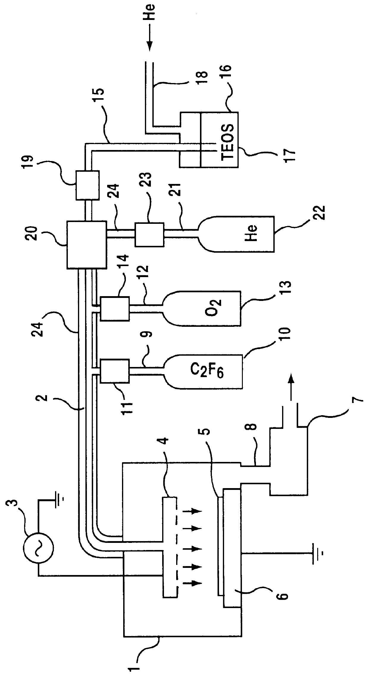
In the first embodiment of the present invention, although the PCVD equipment employing the direct injection method shown in FIG. 1 has been used, another PCVD equipment employing the bubbler us...

fourth embodiments

SECOND TO FOURTH EMBODIMENTS

First, fundamental manufacturing methods as the basis of second to fourth embodiments of the present invention will be explained with reference to FIGS. 12 to 14.

FIG. 12 is a schematic view showing a configuration of another plasma chemical vapor deposition equipment (PCVD equipment) for use in the present invention.

This PCVD equipment has the same basic configuration as that shown in FIG. 1, but it has many kinds of reaction gas to be used in contrast to that shown in FIG. 1. In FIG. 12, like reference numerals in FIG. 1 designate like parts in FIG. 1.

In addition to the material gases used in the equipment in FIG. 1, additional material gases are added as described in the following, and pipings for supplying these material gases are connected to the material gas supply piping 2. Only required material gases may be supplied to the reaction chamber 1 via the material gas supply piping 2. Merely different portions from those in FIG. 1 will be explained here...

fourth embodiment

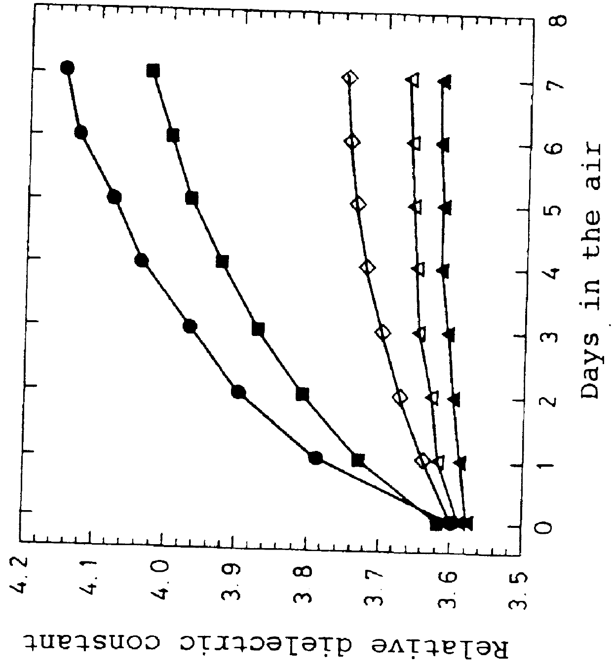
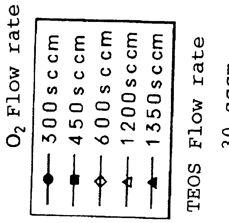
Next, the second to fourth embodiment will be explained with reference to FIGS. 15 to 20 wherein the relative dielectric constant is stabilized by changing film forming conditions to control the density of the SiOF film while measuring a change with the passage of time of the relative dielectric constant.


PUM

PropertyMeasurementUnit
densityaaaaaaaaaa
flow rateaaaaaaaaaa
flow rateaaaaaaaaaa

Abstract

The present invention relates to a method for forming an insulating film with a low relative dielectric constant. A method for forming an insulating film in terms of a plasma chemical vapor deposition, characterized in that a Si supply gas, an oxygen supply gas, and a fluorine supply gas are used a material gas to form said insulating film, and said insulating film is formed under a film forming condition that a density of said insulating film to be formed is equal to or more than 2.25 g/cm3.

Description

1. Field of the InventionThe present invention relates to a method for forming an insulating film and a semiconductor device and, more particularly, a method for forming an insulating film used as an interlayer insulating film of a high integration density semiconductor integrated circuit device and having a low relative dielectric constant and a semiconductor device employing the insulating film therein.2. Description of the Prior ArtIn recent, reconsideration of interlayer insulating films for use in multilayered interconnections has been effected from a view point of high integration density or high speed operation of semiconductor integrated circuit devices.More particularly, from view points of stability, easiness of film forming, etc., an SiO.sub.2 film has been widely used as an interlayer insulating film of the semiconductor integrated circuit device. But the problem of increase in parasitic capacitance has arisen according to progress of recent miniaturization of the circui...

Claims


Application Information

Patent Timeline
Patent Type & Authority Patents(United States)
IPC IPC(8): C23C16/40H01L21/02H01L21/316H01L21/31
CPCC23C16/401H01L21/0212H01L21/02131H01L21/02211H01L21/02216H01L21/02274H01L21/31629H01L21/31
Inventor KUDO, HIROSHISHINOHARA, RIKA
Owner FUJITSU SEMICON LTD
Why Eureka
Try Eureka