Sub-quarter-micron copper interconnections with improved electromigration resistance and reduced defect sensitivity

a sub-quarter-micron copper and interconnection technology, applied in the field of semiconductor manufacturing, can solve the problems of inconvenient use of physical vapor deposition (pvd) methods such as sputtering or evaporation to fill such narrow holes and trenches, hard metal particles removed by polishing tend to abrade metal lines, and cvd copper suffers from limited shelf life of the highly complex precursors required

Inactive Publication Date: 2000-05-30
GLOBALFOUNDRIES INC
View PDF31 Cites 224 Cited by
  • Summary
  • Abstract
  • Description
  • Claims
  • Application Information

AI Technical Summary

Problems solved by technology

It is well known in the art that the use of Physical Vapor Deposition (PVD) methods such as sputtering or evaporation to fill such narrow holes and trenches is not suitable because a highly tapered cross section of the filled metal lines or studs is formed.
Further, during the chemical-mechanical polishing step in this capping process, the hard metal particles removed by polishing tend to abrade the metal line.
However, it has been found that CVD copper suffers from limited shelf life of the highly complex precursors required.
A more serious problem with CVD copper is the contamination of manufacturing line by vapors of copper precursor, which poison the semiconductor devices.
Because the copper seed layer may form up to 20% of the cross-sectional area of an interconnect line, this seed layer seriously hampers the electromigration characteristic of copper interconnection.
Whereas the electromigration resistance of copper is high enough to sustain the wear-out in normally designed conductor lines, defect-induced electromigration failures have been observed in the PVD seed layer/electroplated copper conductor lines.
Understandably, current density in these regions is considerably high during actual

Method used


Image

  • Sub-quarter-micron copper interconnections with improved electromigration resistance and reduced defect sensitivity
  • Sub-quarter-micron copper interconnections with improved electromigration resistance and reduced defect sensitivity
  • Sub-quarter-micron copper interconnections with improved electromigration resistance and reduced defect sensitivity

Examples


Embodiment Construction

)

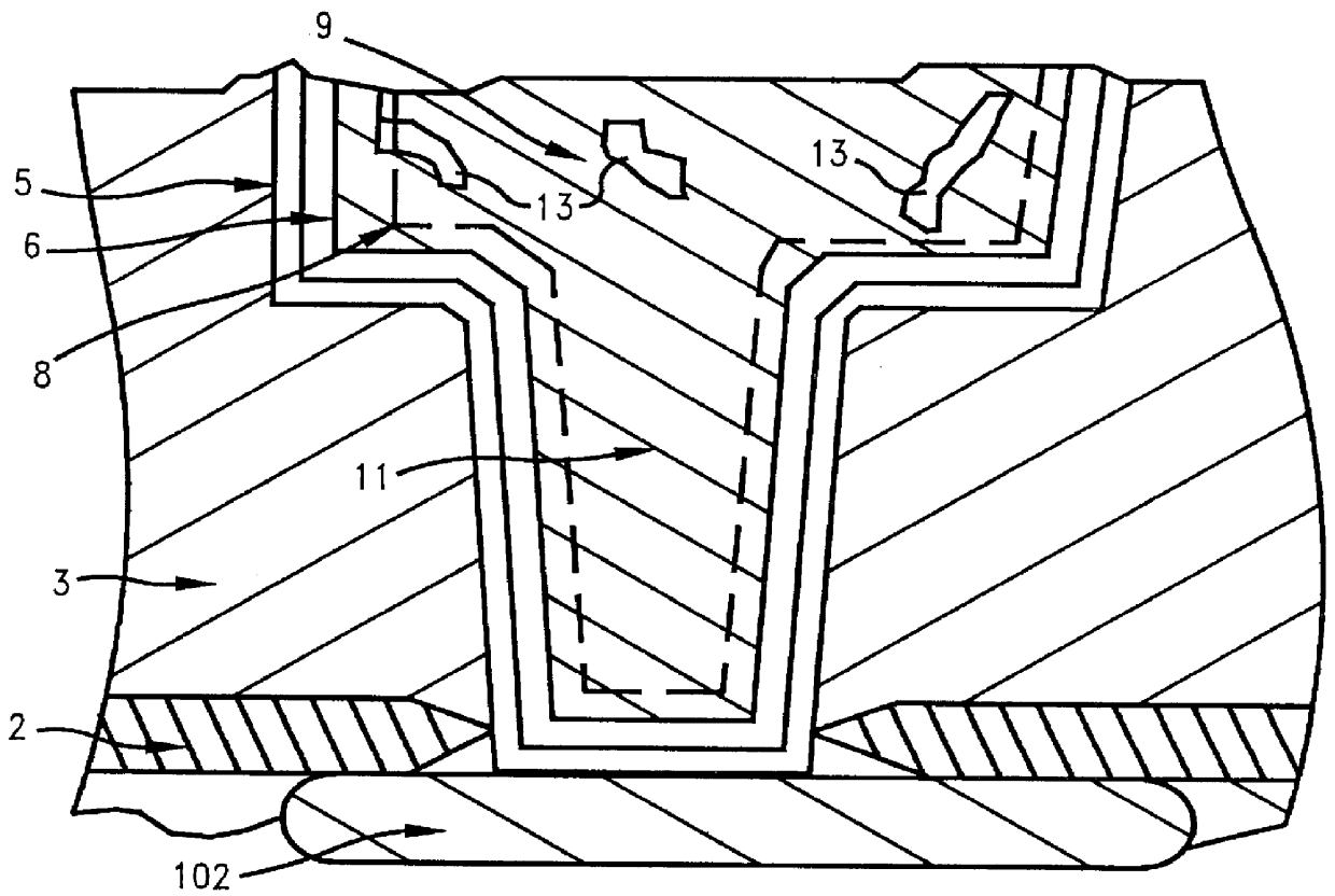
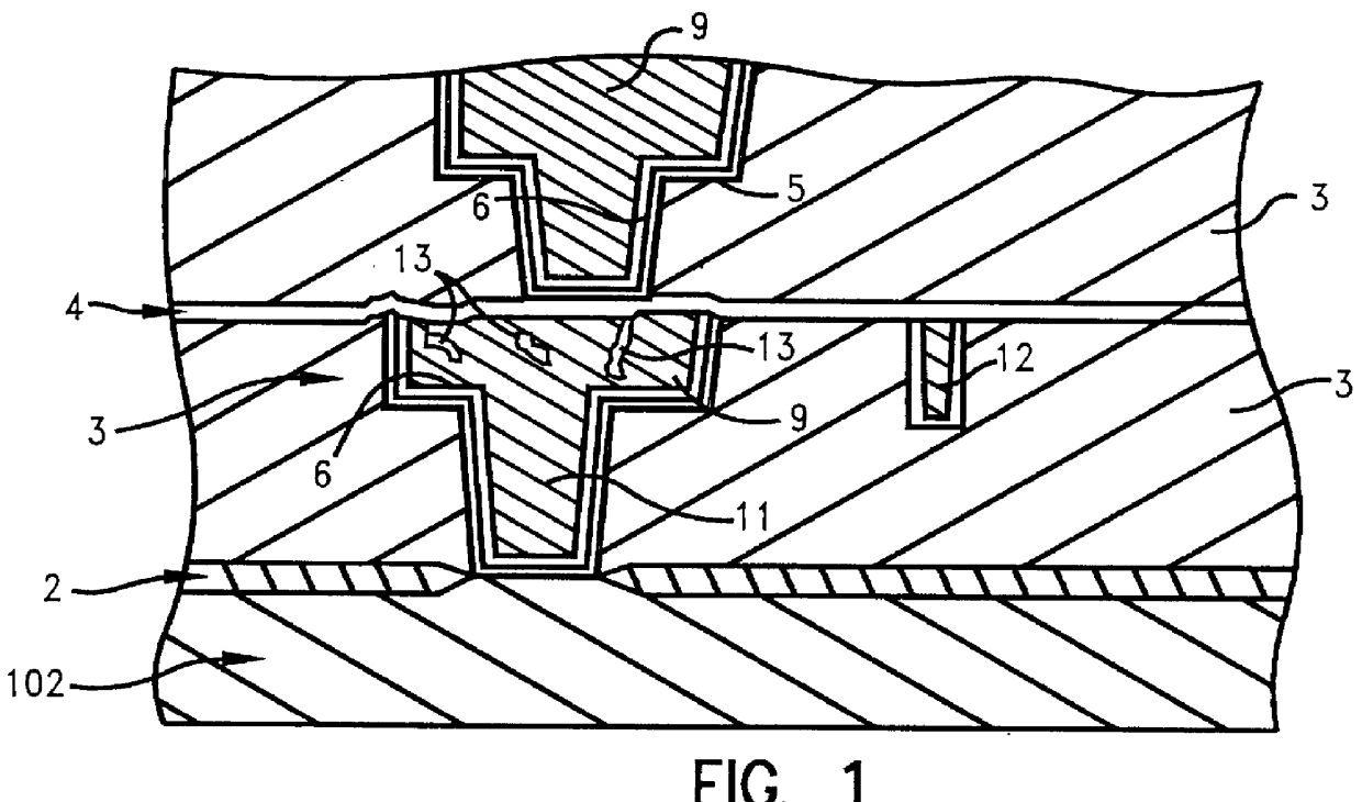
In describing the preferred embodiment of the present invention, reference will be made herein to FIGS. 2-8 of the drawings in which like numerals refer to like features of the invention. Features of the invention are not necessarily shown to scale in the drawings.

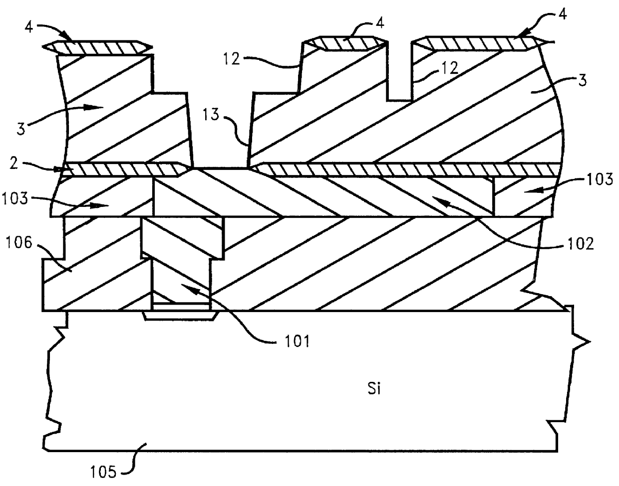
Referring to FIG. 2, there is shown a cross-section of conventional silicon semiconductor structure comprised of a silicon substrate 105 having thereon various device contact studs (vias) 101 and local interconnects (lines) 102, typically tungsten with underlayers of titanium and titanium nitride (not shown) formed within insulator layers 106, 103, respectively. The use of a thin layer of an insulator to prevent the formation of metal spikes between vias and lines, e.g., due to misalignment, is disclosed in U.S. patent application Ser. No. 08 / 947,244 entitled "SELF-ALIGNED COMPOSITE INSULATOR WITH SUB-HALF MICRON MULTILEVEL HIGH DENSITY ELECTRICAL INTERCONNECTIONS AND PROCESS THEREOF" filed on even date herewith.

The metho...


PUM

PropertyMeasurementUnit
Thicknessaaaaaaaaaa
Dielectric polarization enthalpyaaaaaaaaaa
Electrical resistanceaaaaaaaaaa

Abstract

A method of providing sub-half-micron copper interconnections with improved electromigration and corrosion resistance. The method includes double damascene using electroplated copper, where the seed layer is deposited by chemical vapor deposition, or by physical vapor deposition in a layer less than about 800 angstroms.

Description

1. Field of the InventionThe present invention relates to the field of semiconductor manufacturing and, more specifically, to the design of copper based interconnections in sub-micron dimensions with reduced sensitivity for corrosion and defects, and thereby, with improved reliability. The invention also relates to providing methods for forming the designed structure.2. Description of Related ArtAs device geometry continues to scale down for Ultra Large Scale Integrated circuits, there is a growing demand for an interconnect wiring with minimum pitch and high conductivity, and, for a passivation material with a low dielectric constant, while requiring a more robust reliability than ever before. In particular, in the regime of sub-quarter micron line width, the factors of paramount importance are high electrical conductivity and high electromigration resistance.One approach has been to use copper metallurgy, for its high conductivity and high electromigration resistance, along with p...

Claims


Application Information

Patent Timeline
IPC IPC(8): H01L21/768H01L21/70H01L21/3205H01L23/52
CPCH01L21/76846H01L21/76847H01L21/76849H01L21/76877H01L21/76867H01L21/76873H01L21/76858H01L21/283
Inventor RATHORE, HAZARA S.DALAL, HORMAZDYAR M.MCLAUGHLIN, PAUL S.NGUYEN, DU B.SMITH, RICHARD G.SWINTON, ALEXANDER J.WACHNIK, RICHARD A.
Owner GLOBALFOUNDRIES INC
Why Eureka
Try Eureka