

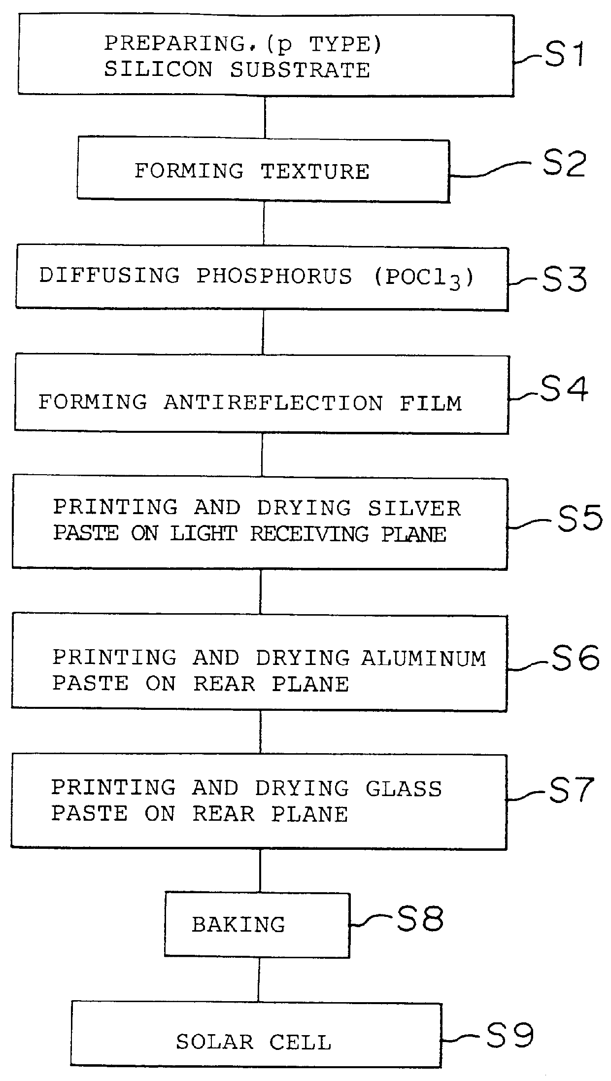
Method of producing a solar cell
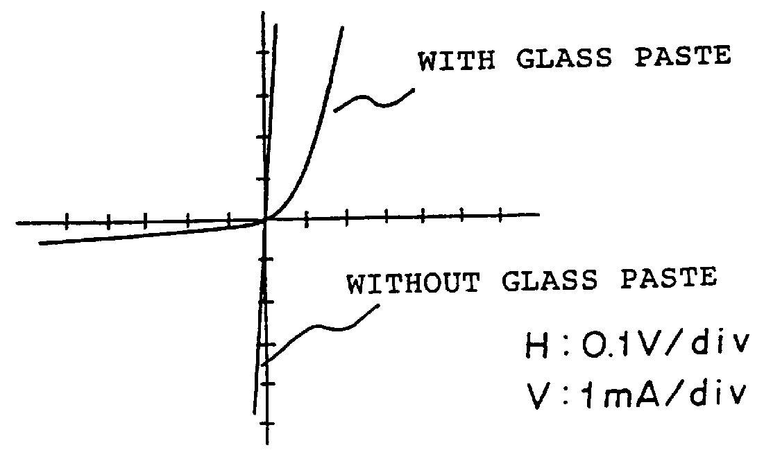
a technology of solar cells and solar energy, applied in the direction of semiconductor/solid-state device manufacturing, electrical apparatus, semiconductor devices, etc., can solve the problems of glass paste removal ability, glass paste removal is easy to be removed, and the energy conversion efficiency of solar cells is remarkably reduced
- Summary
- Abstract
- Description
- Claims
- Application Information
AI Technical Summary
Problems solved by technology
Method used
Image

Examples
embodiment 1
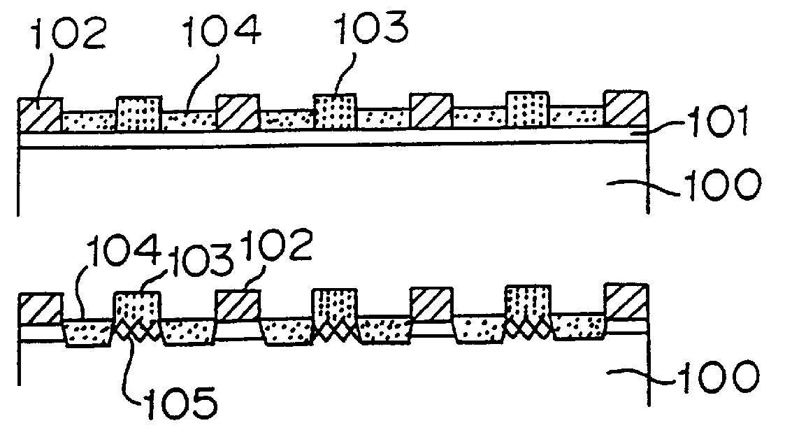
In FIG. 7a, reference numeral 108 designates an n type silicon substrate having a resistivity of about 2 .OMEGA. / cm and numeral 109 designates a p type diffusion layer formed by thermally diffusing boron. The p type diffusion layer 109 may be a p type silicon layer which is formed by ion implantation of an impurity such as boron or by decomposing a gas mixture of a silane type gas and diborane gas (B.sub.2 H.sub.6) by applying an external energy such as heat or plasma. When the diffusion layer 109 is from several hundred .ANG. to several microns thick, it is possible to provide the effect as described below in the same reason as described with respect to
embodiment 2
First, on the p type silicon layer 109, a glass paste 109 is formed in a pattern by screen printing. The shape of the pattern and the pitch may be the same as described in
FIG. 7b illustrates that the glass paste 104, which has been subjected to the baking step, is removed by etching with hydrofluoric acid. Due to the nature of the glass paste 104, etching is obtainable regardless of the electric conductive type of the silicon layer to be treated whether n or p, with the resultant shape as shown in FIG. 7b being obtainable. Reference 110 designates an n type silicon substrate surface exposed as a result of the penetration by the glass paste 104.
FIG. 7c illustrates that the silver paste pattern for forming a n type electrode 102 is printed on the n type silicon substrate surface 110 and the aluminum-silver paste pattern for forming a p electrode 103 is printed on the partly remaining p type diffusion layer 109 and baked.
FIG. 7d illustrates that the aluminum-silver paste for forming a ...
embodiment 6
FIGS. 8a and 8b are respectively a cross-sectional view and a perspective view partly omitted which show the construction of a solar cell according to Embodiment 6 of the present invention.
The structure shown in FIG. 8 is different from those of Embodiments 2 to 5. The feature of this embodiment is to use a p type silicon substrate 112 in which viaholes 113 are provided. The n type diffusion layer 101 is extended to the side plane (inner wall) of the viaholes 113 whereby an electric current generated therethrough is collected by means of the n electrode 102 and the p electrode 103 disposed at the rear plane of the solar cell.
The reason for using such a structure is as follows. When the p type silicon substrate 112 which contributes generation of power is made thin, reduction of the electric current to be produced can not be avoided. Accordingly, all the electrodes are disposed on the rear plane to thereby increase the surface area for receiving light, with the result of increasing a...
PUM
 Abstract
Description
Claims
Application Information