Referring now to the drawing, preferred embodiments of the present invention are described below.
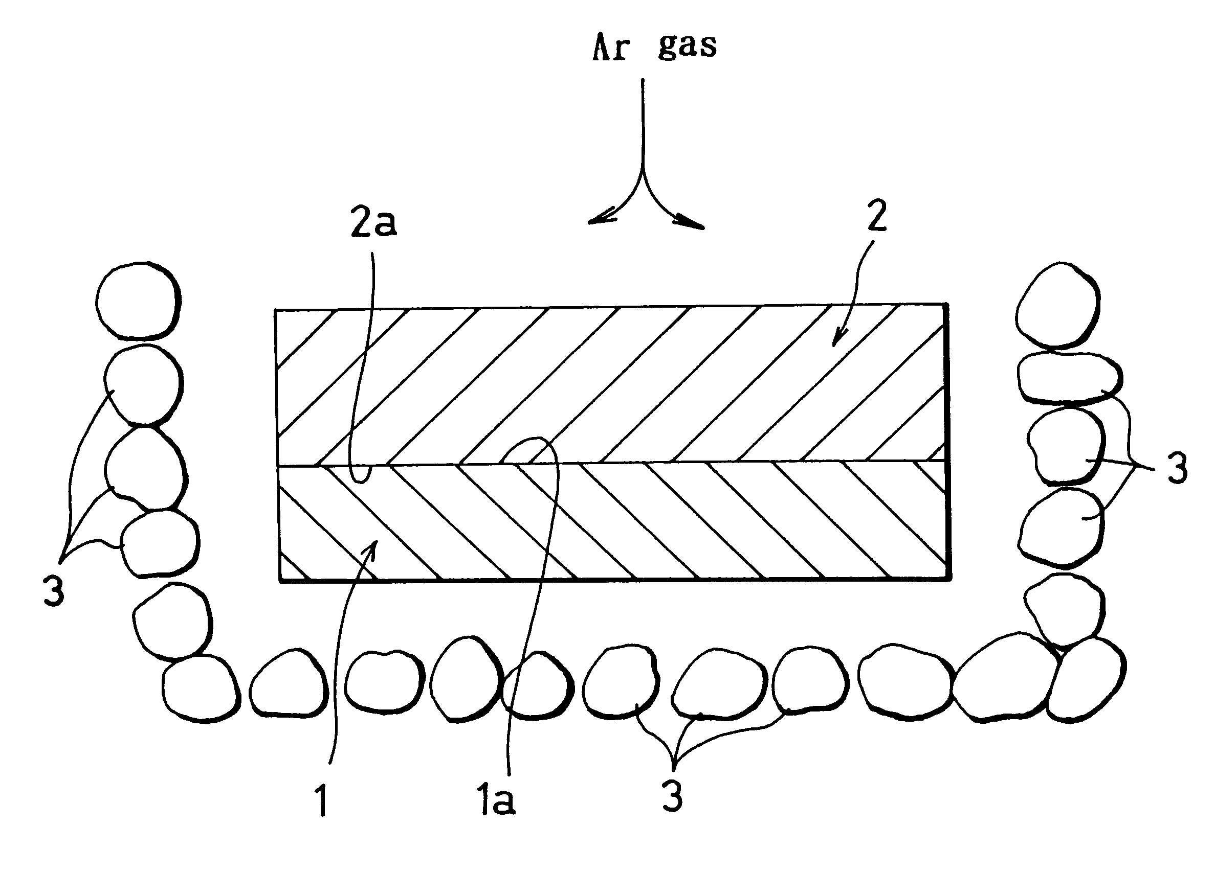
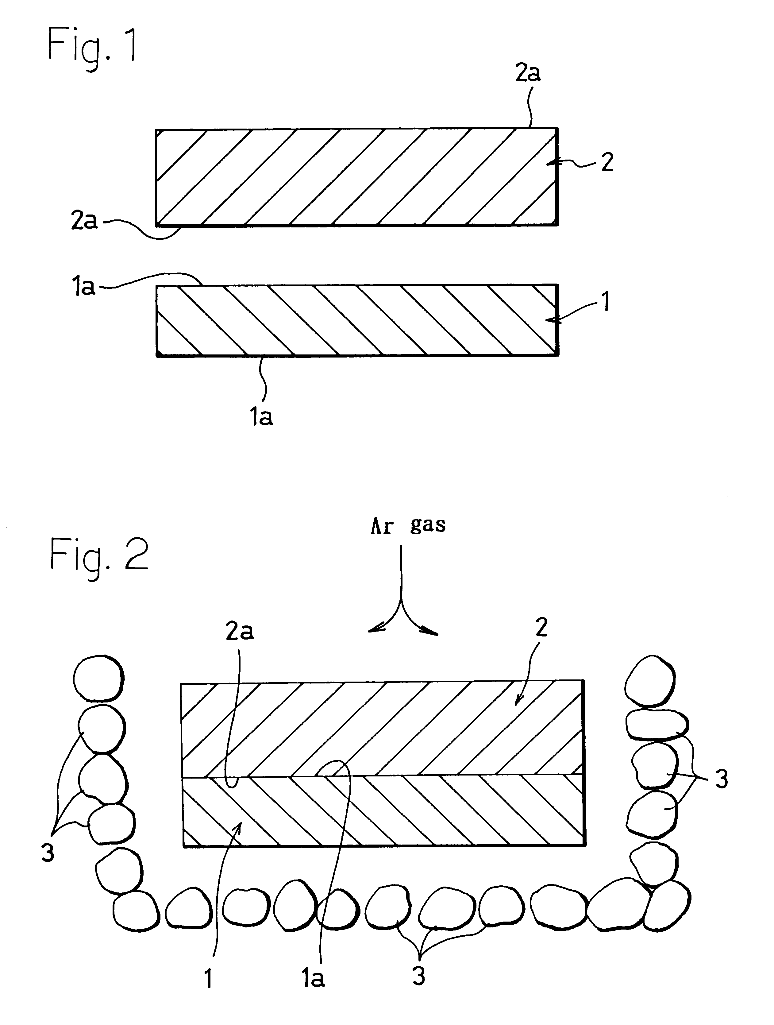
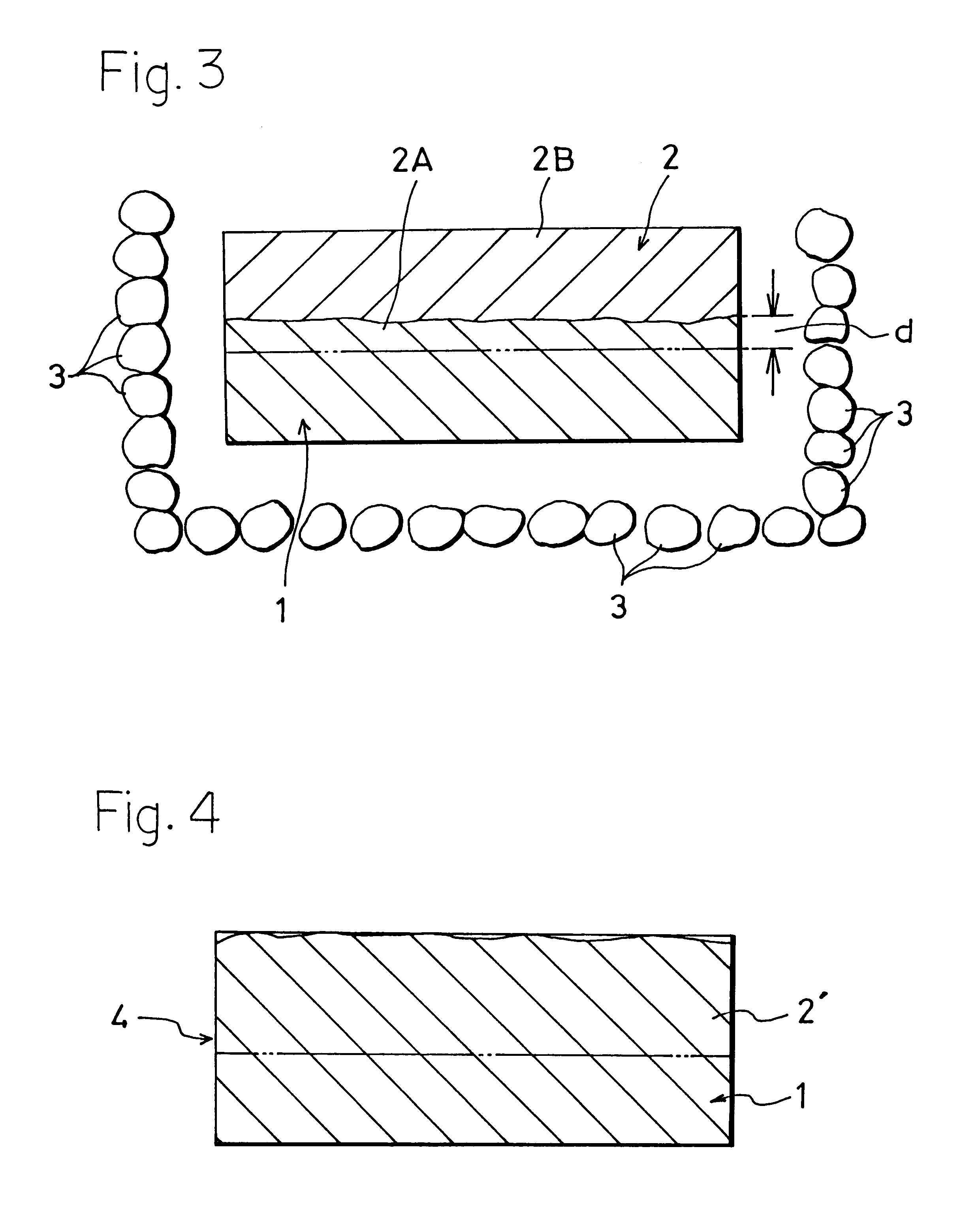
FIG. 1 is a diagram of a material employed in producing a single crystal SiC according to the present invention. In FIG. 1, 1 designates a single crystal hexagonal .alpha.-SiC substrate (6H type or 4H type), which is formed so as to have each plate-shaped SiC, in cutting out numbers of plate-shaped single crystal SiC pieces 1A from a single crystal .alpha.-SiC lump 1' produced by the Acheson method as shown in FIG. 5 and U.S. Pat. No. 4,419,336 and U.S. Pat. No. 4,686,032, top and back surfaces 1a, 1a thereof are processed, thereby being formed so as to have a thickness of 0.5 mm, so that (0001) surface of each plate-shaped single crystal SiC piece 1A may function as a vertical axis.
2 designates a polycrystalline cubic .beta.-SiC plate produced separately by thermal chemical vapor deposition (hereinafter referred to as thermal CVD) at a temperature in a range of 1300 to 1900.degree. C. In the polycrystalline .beta.-SiC plate 2, a .beta.-SiC film having a thickness of substantially 1 mm, whose (111) surface is highly orientated is produced on a sintered graphite not shown in the figure by thermal CVD. Thereafter, the graphite is incinerated for removal, thus isolating both surfaces 2a, 2a of a flat plate-shaped material having a thickness of 0.8 mm, which are ground so as to achieve a smooth surface equal to or lower than 1,000 angstroms RMS, preferably 50 angstroms RMS.
The flat plate-shaped polycrystalline .beta.-sic plate 2 and the single crystal and the single crystal .alpha.-SiC substrate 1 produced in the above way, are washed by a solvent, a supersonic wave, or hydrofluoric acid so as to dry them, before both substrate and plate 1, 2 are laminated to each other for fixation so as to be closely fitted.
In such a state, as shown in FIG. 2, the single crystal .alpha.-SiC substrate 1 and the polycrystalline .beta.-sic plate 2 which are laminated to each other for fixation are horizontally inserted and arranged inside a carbon resistance-heat furnace (not shown) , single crystal .alpha.-SiC grains 3 are arranged and filled at a periphery thereof. An inert gas flow such as Ar is injected into the furnace to the extent of 1 atom, so that a temperature of a center of the furnace is raised from 1,100.degree. C. up to 2,000 to 2,300.degree. C. at an average velocity by taking 10 hours, and it is kept at 2,000 to 2,300.degree. C. for substantially 5 hours. Thus, a first heat treatment is applied thereto under an inert gas atmosphere and a saturated SiC vapor atmosphere.
By this first heat treatment, as shown in FIG. 3, the polycrystalline .beta.-SiC plate 2 is solid-phase-transformed, thus leading to single crystallization of the polycrystalline .beta.-SiC plate portion 2A, whose depth range d is 100 to 50 .mu.m all over a layer surface.
After first heat treatment, the heat treatments are repeated under the same atmosphere and temperature conditions as the above mention, whereby the above single-crystallized portion 2A is solid-phase grown as a seed crystal, thereby transforming the rest of the polycrystalline .beta.-SiC plate portion 2B into single crystals so as to lead to the single crystal portion 2' oriented in the same direction as the crystal axis of the single crystal .alpha.-SiC substrate 1. Consequently, the single crystal portion 2' is integrated with the single crystal of the single crystal .alpha.-SiC substrate 1, thereby growing them into a large sized single crystal SIC 4 as shown in FIG. 4.
In the above embodiment, the opposite faces 1a, 2a of the single crystal .alpha.-Sic substrate 1 and the polycrystalline .beta.-SiC plate 2 are ground so as to have smooth surfaces equal to or lower than 1,000 angstroms RMS, preferably, 50 angstroms RMS. Under a condition wherein the smooth surfaces are closely laminated all over the mutual surfaces, they are subjected to a heat treatment. Alternatively, even though both opposed surfaces 1a, 2a are not strictly closely fitted, and the opposed surfaces 1a, 2a are not entirely finished as the flat surfaces so that they are not completely contacted to each other, only a partial contact point advances single crystallization owing to solid-phase transformation to a surface direction wherein the contact point is a starting point, whereby a whole of the polycrystalline .beta.-SiC plate 2 is single-crystallized. This has been confirmed by an experiment.
Therefore, it does not require a troublesome and expensive preliminary process wherein the single crystal .alpha.-SiC substrate 1 and the polycrystalline .beta.-SiC plate 2 are ground resulting in the high accurate smooth surfaces so that the opposed surfaces 1a, 2a may be strictly closely fitted, or they are finished to be smooth so that the whole surfaces may be completely fitted to each other. The single crystal .alpha.-SiC substrate 1 and the polycrystalline .beta.-SiC plate 2 having low accurate smooth surfaces are used, and the both substrate and plate 1, 2 are simply laminated each other for fixation so as to apply heat treatment thereto, a whole area of the polycrystalline .beta.-SiC plate 2 is single-crystallized, whereby it is possible to produce single crystal SiC having high quality with high productivity, which are substantially free from lattice defects and micropipe defects.
As the polycrystalline SiC plate, as shown in the above embodiment, the plate-shaped SiC produced by thermal chemical vapor deposition is employed, which the polycrystalline SiC plate itself has high purity and no defects such as a void. Therefore, between the single crystal SiC substrate and the polycrystalline SiC plate, crystal grain boundaries or the like are not formed, thus enhancing the quality of single crystal SiC further. However, it is not limited to the above. Alternatively, a plate-shaped SiC produced by an ion plating method, spattering method and plasma CVD may be used.
Moreover, as shown in the above embodiment, preferably, single crystal .alpha.-SiC is used as the single crystal SiC substrate. Alternatively, the single crystal .beta.-SiC may be used. Especially, in case of employing the single crystal SiC substrate having a crystal surface opposed to the polycrystalline SiC plate, which is (0001) surface .+-.5.degree. or (110) surface .+-.5.degree. of the single crystal SiC piece cut out in a plate shape from the single crystal SiC lump produced by the Achison method, the single crystal is grown from the crystal surface of the single crystal SiC substrate to a C axial direction by solid-phase transformation of the polycrystalline SiC plate accompanied with the heat treatment. In the growing step, introduction of crystal defects are extremely reduced, thereby growing the crystal of the same polymorphous structure as the single crystal SiC substrate easily and surely. As a result, the high quality single crystal SiC in which another polymorphous structure is not mixed can be efficiently obtained.
Furthermore, the single crystal .alpha.-SiC substrate 1 employed in the above embodiment may be either of a single crystal 6H-SiC or a single crystal 4H-SiC. Moreover, in the above embodiment, the polycrystalline .beta.-SiC film 2 as the polycrystalline plate is employed. Alternatively, even though an amorphous plate having high purity (equal to or less than 10.sup.14 atm/cm.sup.3) is employed, the single crystal SiC having high quality similar to the above one can be obtained.