Multilayer thin film

a thin film, multi-layer technology, applied in the direction of superconductor devices, natural mineral layered products, instruments, etc., can solve the problems of difficult to obtain a film, difficult to provide good device characteristics, and awkward formation of perovskite layers

Inactive Publication Date: 2001-07-10
SNAPTRACK
View PDF8 Cites 92 Cited by
  • Summary
  • Abstract
  • Description
  • Claims
  • Application Information

AI Technical Summary

Problems solved by technology

With omnidirectionally oriented polycrystalline materials, it is difficult to provide good device characteristics on account of the disturbances of physical quantities.
However, since the perovskite oxide thin film is likely to have tetragonal (110) orientation or tetragonal (101) orientation on the above buffer layer, it is difficult to obtain a film in which the tetragonal (001) face or rhombohedral (111) face vertical to the axis of polarization is oriented.
However, the perovskite layer is awkward to form, and it is particularly difficult to form a homogeneous perovskite layer having a composition as designed.

Method used


Image

  • Multilayer thin film
  • Multilayer thin film
  • Multilayer thin film

Examples


first embodiment

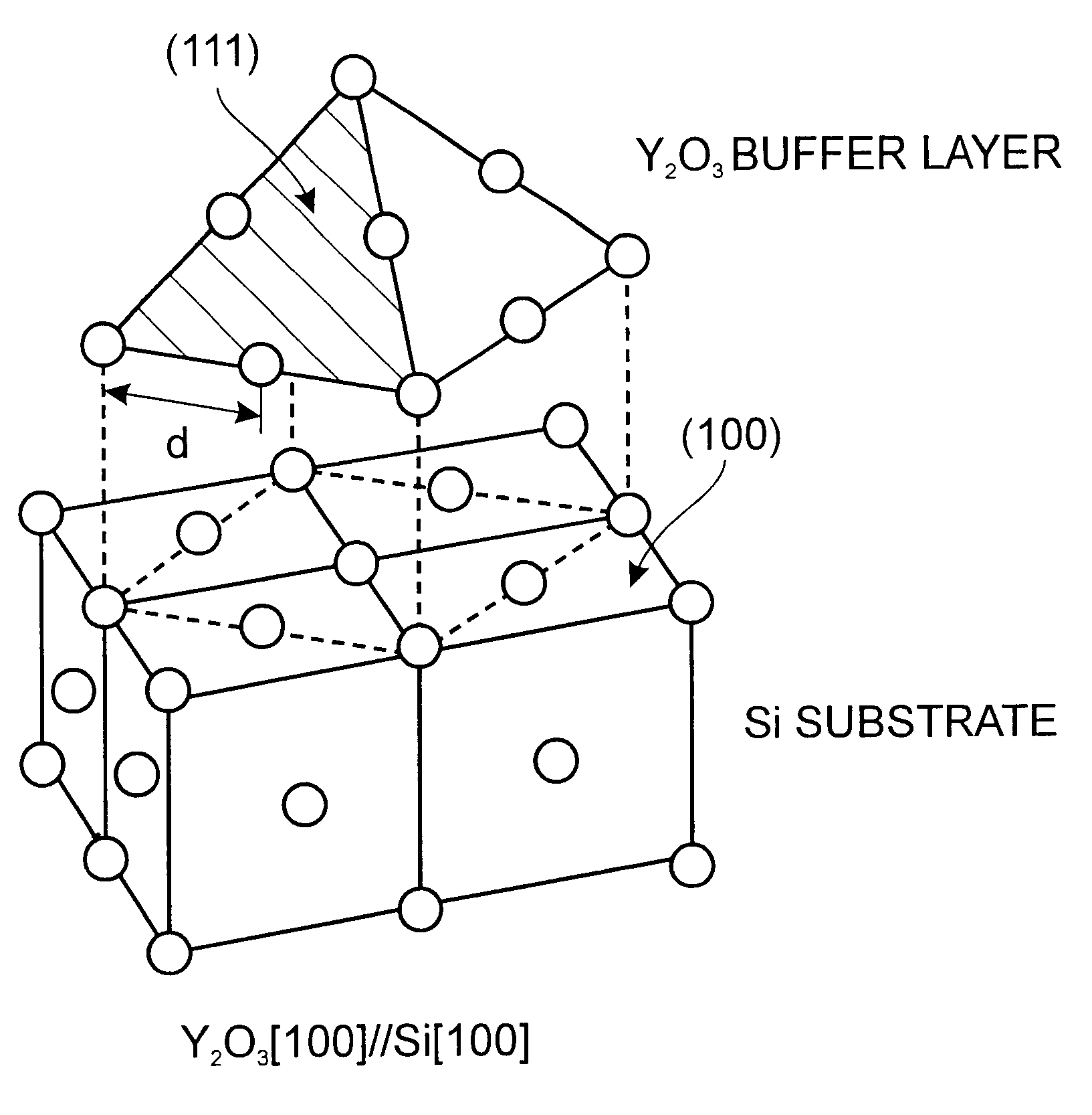
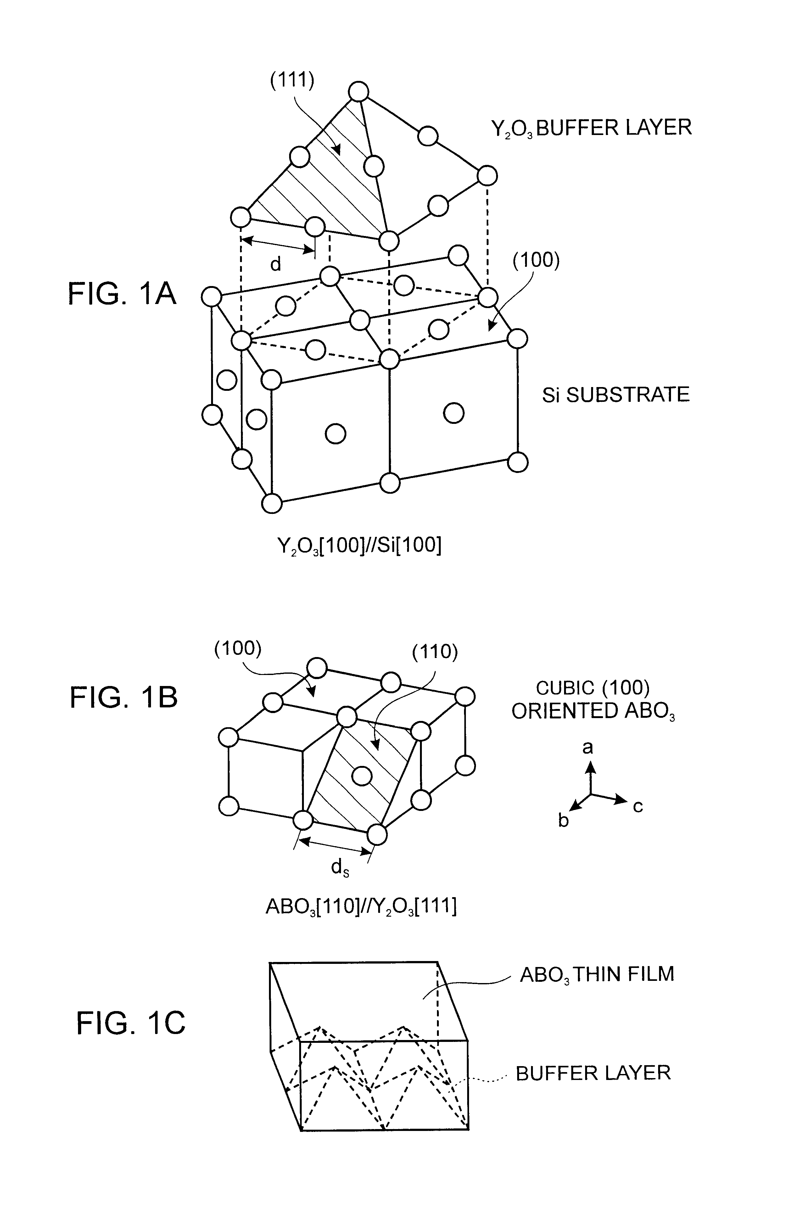
The buffer layer interleaved between the perovskite oxide thin film and the substrate is characterized in that the interface between the buffer layer and the perovskite oxide thin film is defined by a {111} facet plane. FIG. 1A is a schematic view depicting the surface of the buffer layer formed on an Si (100) single crystal substrate. While the buffer layer shown is composed of Y.sub.2 O.sub.3, it is understood that oxygen atoms are not shown in FIG. 1A. In the invention, the buffer layer is a cubic (100) oriented, tetragonal (001) oriented or monoclinic (001) oriented epitaxial film, and so the facet plane shown is the {111} facet plane.

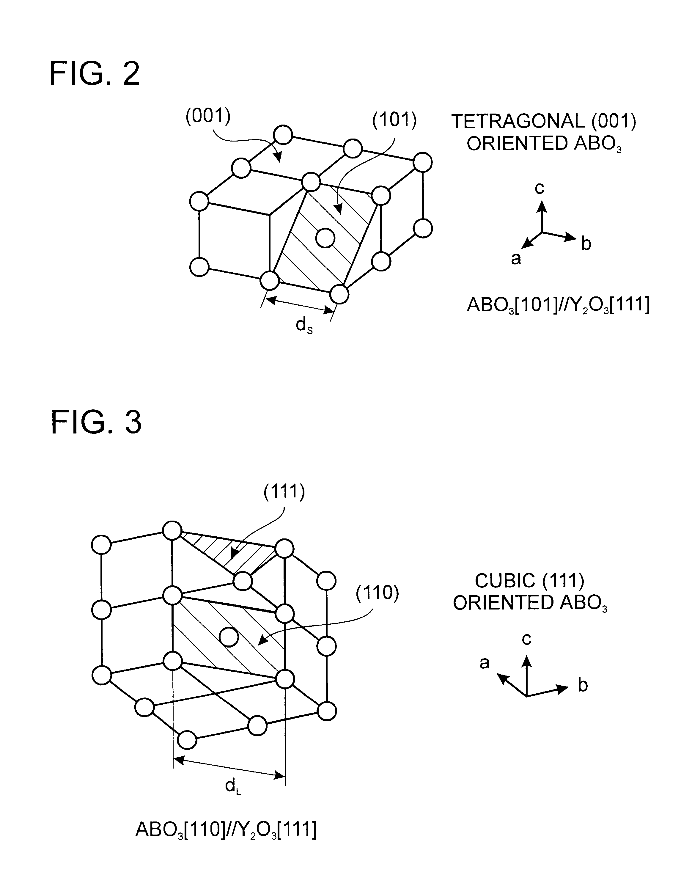
In the multilayer thin film according to this embodiment, substantially parallel to the {111} facet plane of the buffer layer there is present a {110} face of a cubic, rhombohedral, tetragonal or orthorhombic crystal of the perovskite oxide thin film, a {101} face of the tetragonal or orthorhombic crystal or a {011} face of the orthorhombic crystal...

second embodiment

In the second embodiment of the invention, the buffer layer is located between the metal thin film and the substrate. It is here noted that the buffer layer also functions as an insulator.

The buffer layer according to this embodiment is characterized in that the interface between the buffer layer and the metal thin film includes a {111} facet plane. FIG. 4A is a schematic view depicting the facet planes on the surface of the buffer layer, and FIG. 4B is an exaggerated view of some facet planes. The buffer layer according to the second embodiment is the same as that according to the first embodiment, and is an epitaxial film of cubic (100) orientation, tetragonal (001) orientation or monoclinic (001) orientation; that is, the facet plane is the {111} facet plane. The metal thin film, in a {111} oriented film form, grows epitaxially on the {111} facet planes of the buffer layer. As the metal thin film grows, depressions defined by the facet planes are filled up. Finally, the surface o...

example

Example 1 (First Embodiment)

A multilayer thin film comprising a ZrO.sub.2 thin film, a Y.sub.2 O.sub.3 thin film, and a PbTiO.sub.3 thin film stacked on an Si (100) single crystal substrate in this order was prepared according to the following procedure.

First, an Si single crystal wafer (in a disk form of 2 inches in diameter and 250 .mu.m in thickness) was provided, which was cut and mirror polished so that its surface was defined by a (100) face. The surface of this wafer was cleaned by etching with a 40% aqueous solution of ammonium fluoride.

Then, the single crystal substrate 2 was fixed to the substrate holder 3 located in the vacuum chamber 1a in the evaporation system 1 shown in FIG. 14, and equipped with rotating and heating mechanisms. The vacuum chamber was evacuated to a vacuum of 10.sup.-6 Torr by means of an oil diffusion pump. To protect the cleaned surface of the substrate with an Si oxide, the substrate was rotated at 20 rpm and heated to 600.degree. C. while oxygen w...


PUM

PropertyMeasurementUnit
thicknessaaaaaaaaaa
sizeaaaaaaaaaa
sizeaaaaaaaaaa

Abstract

The first object of the invention is to provide means that enables a perovskite oxide thin film having (100) orientation, (001) orientation or (111) orientation to be easily obtained, and the second object of the invention is to provide a multilayer thin film comprising a unidirectionally oriented metal thin film of good crystallinity. The multilayer thin film according to the first embodiment of the invention comprises a buffer layer and a perovskite oxide thin film present thereon. The interface between the buffer layer and the perovskite oxide thin film is made up of a {111} facet plane. Substantially parallel to the facet plane there is present a {110} face of a cubic, rhombohedral, tetragonal or orthorhombic crystal of the perovskite oxide thin film, a {101} face of the tetragonal or orthorhombic crystal or a {011} face of the orthorhombic crystal. The multilayer thin film according to the second embodiment of the invention comprises a metal thin film that is a cubic (100) unidirectionally oriented epitaxial film, and a buffer layer where a {111} facet plane is present on the interface of the buffer layer in contact with the metal thin film.

Description

1. Art FieldThis invention relates to a multilayer thin film structure comprising a perovskite oxide thin film or a metal thin film.2. Background ArtElectronic devices have been elaborated which are fabricated by forming various function films such as superconducting, dielectric, ferroelectric or piezoelectric films on silicon substrates or semiconductor crystal substrates, followed by integration. For example, for the combination of semiconductors with superconductors, SQUIDs, Josephson devices, superconducting transistors, electromagnetic wave sensors and superconducting wired LSIs are contemplated. For the combination of semiconductors with dielectric materials, LSIs having a higher degree of integration and dielectric isolated LSIs relying on SOI technology are contemplated. For the combination of semiconductors with ferroelectric materials, non-volatile memories, infrared sensors, optical modulators, optical switches and OEICs (opto-electronic integrated circuits) are contempla...

Claims


Application Information

Patent Timeline
Patent Type & Authority Patents(United States)
IPC IPC(8): B32B15/04C30B23/02
CPCB32B15/04C30B23/02C30B29/32
Inventor NOGUCHI, TAKAOYANO, YOSHIHIKO
Owner SNAPTRACK
Why Eureka
Try Eureka