Display switch with double layered gate insulation and resinous interlayer dielectric

a dielectric and display switch technology, applied in the field of thin film transistors, can solve the problems of difficult to obtain the required crystalinity, difficult to obtain a good annealing effect across the wide area, and the irradiation of laser light is apt to become unstabl

Inactive Publication Date: 2001-11-13
SEMICON ENERGY LAB CO LTD
View PDF189 Cites 92 Cited by
  • Summary
  • Abstract
  • Description
  • Claims
  • Application Information

AI Technical Summary

Problems solved by technology

However, it has been the fact that it is difficult to obtain a required crystalinity across the wide area through the heat treatment because it may cause nonuniformity in the crystallization.
Further, although it is possible to obtain the high crystalinity partly by irradiating laser light, it is difficult to obtain a good annealing effect across the wide area.
In particular, the irradiation of the laser light is apt to become unstable under the condition for obtaining the good crystalinity.
However, it has been also found that because the metal element is contained within the film and the amount thereof to be introduced has t...

Method used


Image

  • Display switch with double layered gate insulation and resinous interlayer dielectric
  • Display switch with double layered gate insulation and resinous interlayer dielectric
  • Display switch with double layered gate insulation and resinous interlayer dielectric

Examples


first embodiment

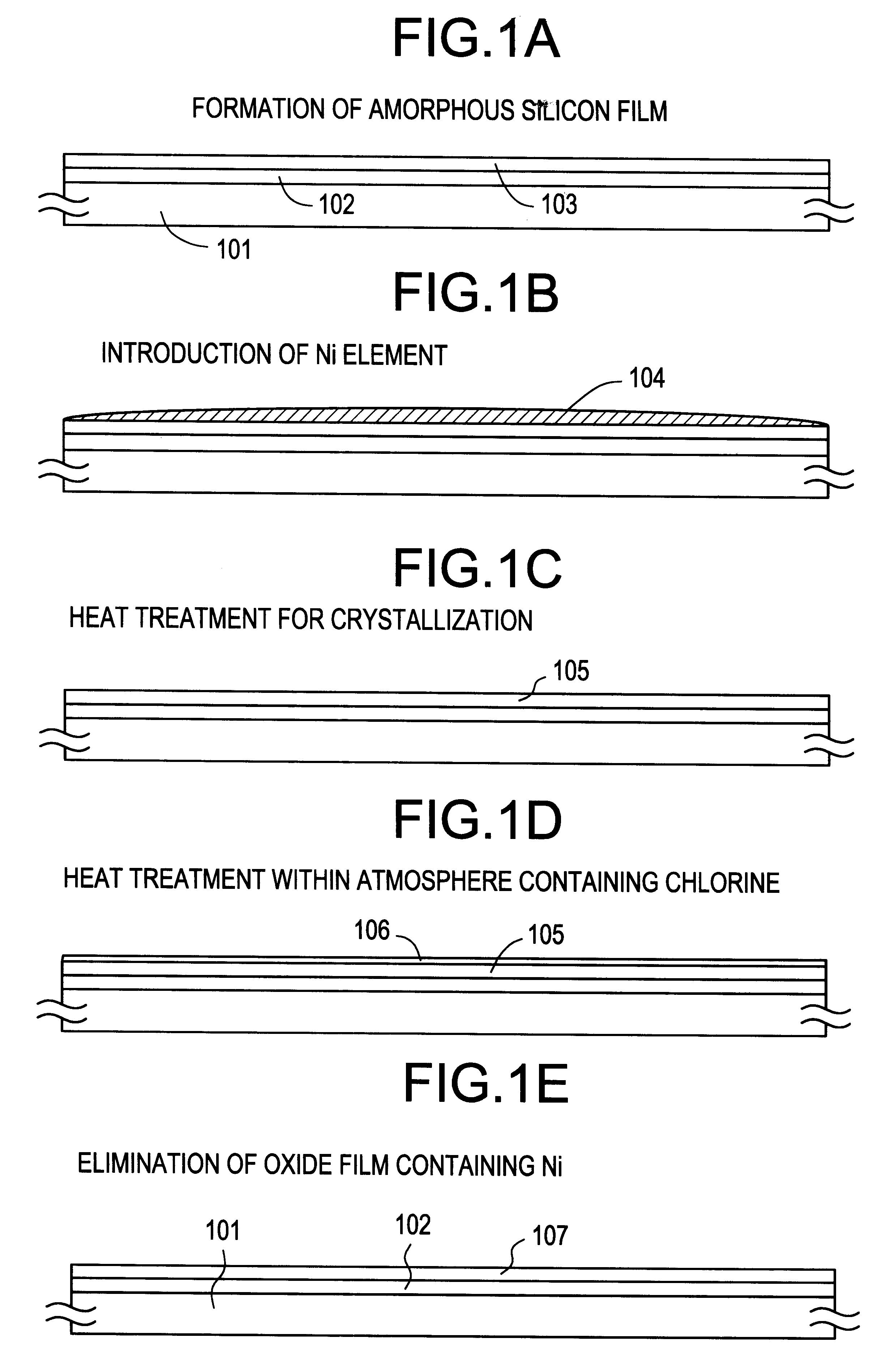
An arrangement for obtaining a crystal silicon film on a glass substrate by utilizing nickel element will be explained in the present embodiment.

At first, the crystal silicon film having a high crystalinity is obtained by an action of nickel element in. the present embodiment.

Next, a thermal oxide film containing halogen element is formed on the crystal silicon film by thermal oxidation. At this time, the nickel element remaining in the crystal silicon film thus obtained is gettered to the thermal oxide film by the action of the halogen element.

Then, the thermal oxide film containing the nickel element in high concentration as a result of the gettering is eliminated. Thereby, the crystal silicon film having nickel element in low concentration while having the high crystalinity is obtained on the glass substrate.

A fabrication process of the present embodiment will be explained by using FIG. 1 below. At first, a silicon oxide nitride film 102 is formed as an underlying film in a thick...

second embodiment

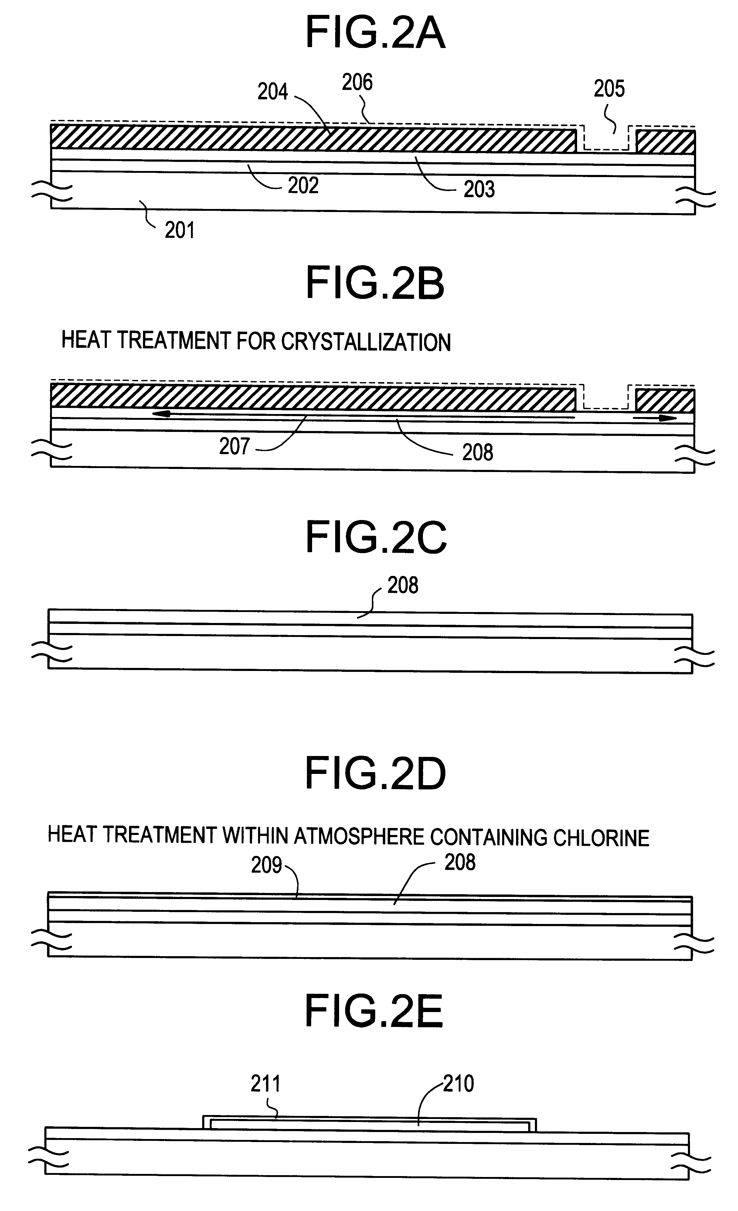
The present embodiment relates to a case when laser light is irradiated after obtaining the crystal silicon film by the heat treatment shown in FIG. 1B in the arrangement shown in the first embodiment to promote the crystallization thereof.

When the temperature of the heat treatment shown in FIG. 1B is low or when the treatment time is short, i.e. when the heating temperature or the heating time is restricted by the reason of the fabrication process, there is a possibility that the required crystalinity cannot not be obtained. In such a case, the required high crystalinity may be obtained by implementing annealing by irradiating laser light.

The width of the permissible laser irradiation condition of the irradiation of laser this time is wide as compared to the case when the amorphous silicon film is directly crystallized. Further, its high reproduciblity may be enhanced.

The irradiation of laser light is implemented after the step shown in FIG. 1C. It is also important to form the amo...

third embodiment

The present embodiment relates to a case when an infrared lamp is used instead of the laser light in the second embodiment. The use of infrared ray allows the silicon film to be heated selectively without heating the glass substrate so much. Accordingly, an effective heat treatment may be implemented without giving thermal damage to the glass substrate.


PUM


Abstract

Concentration of metal element which promotes crystallization of silicon and which exists within a crystal silicon film obtained by utilizing the metal element is reduced. A first heat treatment for crystallization is implemented after introducing nickel element to an amorphous silicon film 103. Then, after obtaining the crystal silicon film, another heat treatment is implemented within an oxidizing atmosphere at a temperature higher than that of the previous heat treatment. At this time, HCl or the like is added to the atmosphere. A thermal oxide film 106 is formed in this step. At this time, gettering of the nickel element into the thermal oxide film 106 takes place. Next, the thermal oxide film 106 is removed. Thereby, a crystal silicon film 107 having low concentration of the metal element and a high crystalinity can be obtained.

Description

1. Field of the InventionThe present invention relates to a semiconductor device typified by a thin film transistor and to a fabrication method thereof. Specifically, the present invention relates to a semiconductor device using a crystal silicon thin film formed on a glass substrate or a quartz substrate and to a fabrication method thereof.2. Description of Related ArtHitherto, there has been known a thin film transistor using a silicon film, i.e. a technology for forming the thin film transistor by using the silicon film formed on a glass substrate or quartz substrate.The glass substrate or quartz substrate is used because the thin film transistor is used for an active matrix type liquid crystal display. While a thin film transistor has been formed by using an amorphous silicon film in the past; it is being tried to fabricate the thin film transistor by utilizing a silicon film having a crystalinity (referred to as "crystal silicon film" hereinbelow) in order to enhance its perfor...

Claims


Application Information

Patent Timeline
IPC IPC(8): H01L29/66H01L21/02H01L21/70H01L21/336H01L21/20H01L21/322H01L27/12H01L29/786H01L21/84H01L29/49H01L29/40H01L21/77
CPCH01L21/2022H01L21/3226H01L27/12H01L27/1203H01L29/66757H01L29/66765H01L29/78621H01L29/78675H01L27/1277H01L29/4908H01L21/02592H01L21/02686H01L21/02488H01L21/02422H01L21/02532H01L21/02598H01L21/0242H01L21/02672
Inventor YAMAZAKI, SHUNPEITERAMOTO, SATOSHIKOYAMA, JUNOGATA, YASUSHIHAYAKAWA, MASAHIKOOSAME, MITSUAKI
Owner SEMICON ENERGY LAB CO LTD
Why Eureka
Try Eureka