Low temperature rapid ramping anneal method for fabricating layered superlattice materials and making electronic devices including same

a superlattice material and low temperature technology, applied in the direction of polycrystalline material growth, crystal growth process, after-treatment details, etc., can solve the problems of deterioration of the electronic characteristics of the mosfet, economic unfeasibility, oxygen damage to the semiconductor substrate and other elements of the cmos circuit,

a superlattice material and low temperature technology, applied in the direction of polycrystalline material growth, crystal growth process, after-treatment details, etc., can solve the problems of deterioration of the electronic characteristics of the mosfet, economic unfeasibility, oxygen damage to the semiconductor substrate and other elements of the cmos circuit,

US6326315B1Inactive Publication Date: 2001-12-04SYMETRIX +1

Image

  • Low temperature rapid ramping anneal method for fabricating layered superlattice materials and making electronic devices including same
  • Low temperature rapid ramping anneal method for fabricating layered superlattice materials and making electronic devices including same
  • Low temperature rapid ramping anneal method for fabricating layered superlattice materials and making electronic devices including same

Examples


example 1

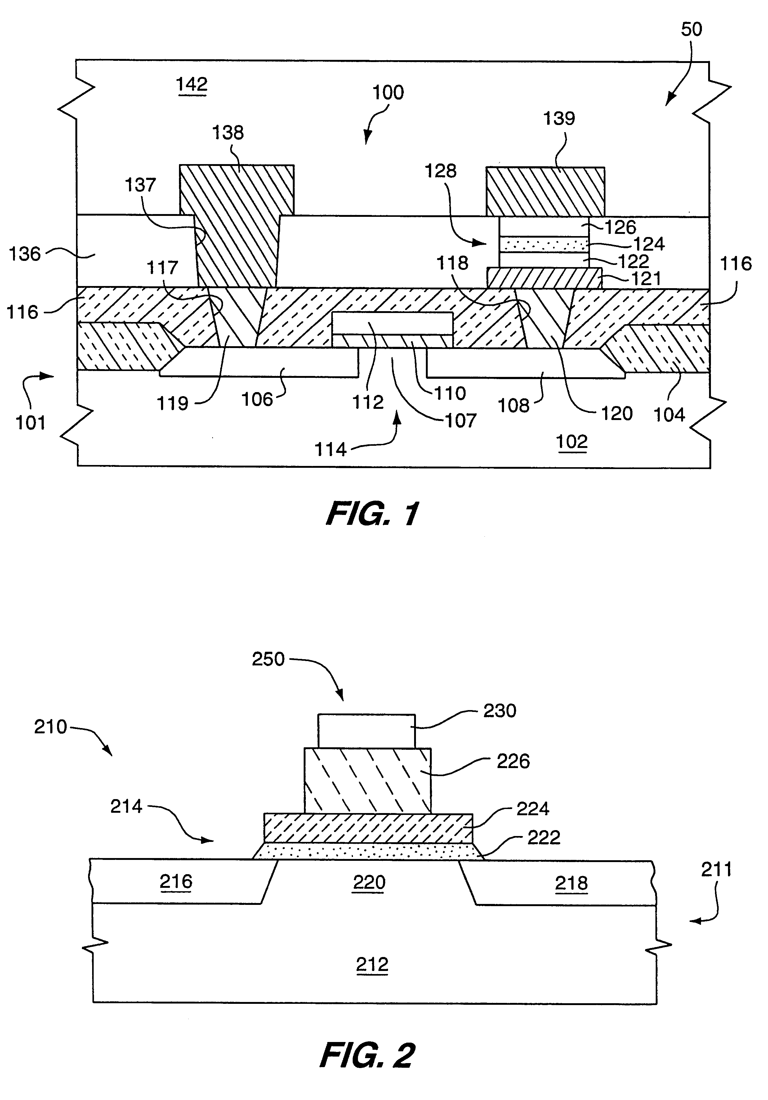
Ferroelectric thin film capacitors, as depicted in FIGS. 4 and 5, containing a thin film of strontium bismuth tantalate layered superlattice material were fabricated in accordance with the invention. The remanent polarizations of the capacitors were measured and compared to study the effects of processing conditions on ferroelectric polarizability.

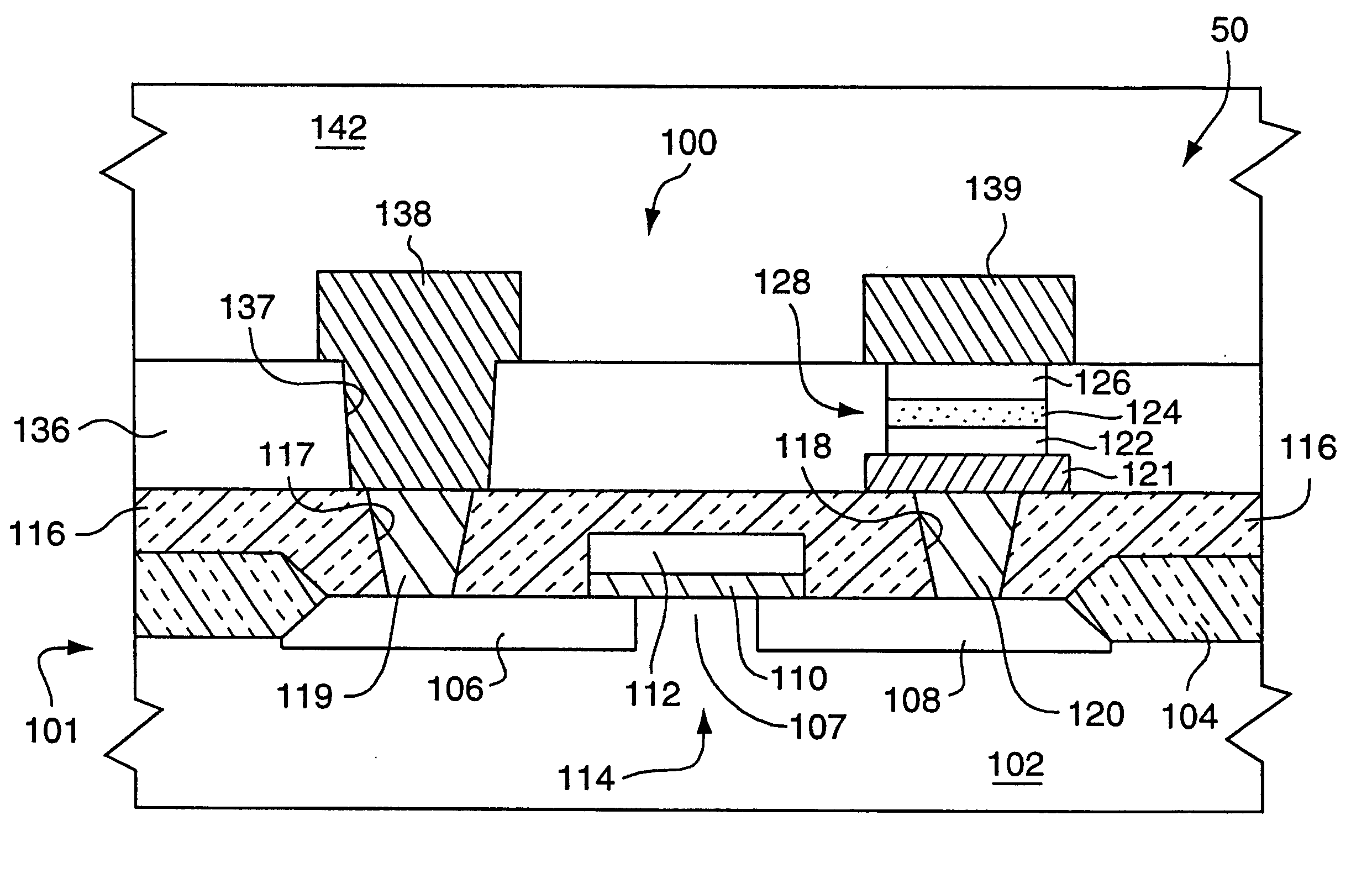
Each of a series of P-type 100 Si wafer substrates 502 was oxidized to form a layer of silicon dioxide 504. The substrate was dehydrated in a vacuum oven at 80.degree. C. for 30 minutes. An adhesive layer 506 consisting substantially of titanium and having a thickness of 100 nm was sputter-deposited on the substrate, using an argon atmosphere, 8 mTorr pressure and 0.53 amps. Then, under similar sputter conditions, a bottom platinum electrode 508 layer having a thickness of 200 nm was deposited. On each wafer, the bottom electrode layer was pre-annealed at 650.degree. C. for 30 minutes in O.sub.2 gas flowing at 6 l / m, using 10 minute push-p...


PUM


Abstract

A liquid precursor for forming a layered superlattice material is applied to an integrated circuit substrate. The precursor coating is annealed in oxygen using a rapid ramping anneal ("RRA") technique with a ramping rate of 50.degree. C. / second at a hold temperature of 650.degree. C. for a holding time of 30 minutes.

Description

BACKGROUND OF THE INVENTION1. Field of the InventionThe invention in general relates to the fabrication of layered superlattice materials, and more particularly to a fabrication method that provides ferroelectric integrated circuit devices containing thin films of layered superlattice materials possessing high-polarizability, low fatigue and low-leakage current characteristics by using a low-temperature rapid ramping anneal.2. Statement of the ProblemFerroelectric compounds possess favorable characteristics for use in nonvolatile integrated circuit memories. See Miller, U.S. Pat. No. 5,046,043. A ferroelectric device, such as a capacitor, is useful as a nonvolatile memory when it possesses desired electronic characteristics, such as high residual polarization, good coercive field, high fatigue resistance, and low leakage current. Layered superlattice material oxides have been studied for use in integrated circuits. U.S. Pat. No. 5,434,102, issued Jul. 18, 1995, to Watanabe et al., a...

Claims


Application Information

Patent Timeline
04 Dec 2001
Publication
US6326315B1
IPC
C30B7/00; H01L21/28; H01L21/02; C01G1/02; C01G35/00; H01L21/316; H01L21/822; H01L21/8246; H01L21/8247; H01L27/04; H01L27/105; H01L29/788; H01L29/792
CPC
C30B7/00; H01L21/28291; C30B29/68; C30B7/005; H01L29/40111; C30B33/02; H10B53/00
Inventors
UCHIYAMA, KIYOSHI; ARITA, KOJI