Method of fabrication of semiconducting compounds of nitrides A3B5 of P-and N-type electric conductivity

a technology of nitride and semiconducting compounds, which is applied in the direction of lasers, crystal growth processes, wave amplification devices, etc., can solve the problems of high concentration of hole type carriers, low resistance of p-type layers, and limited method, and achieves low electric resistance, high structural quality, and high light intensity

Inactive Publication Date: 2001-12-11
INST WYSOKICH CISNIEN POLSKIEJ AKADI NAUK
View PDF2 Cites 49 Cited by
  • Summary
  • Abstract
  • Description
  • Claims
  • Application Information

AI Technical Summary

Benefits of technology

The subject of the Invention relates to the method of fabrication of nitride semiconductors A.sub.3 B.sub.5 such as GaN, AIN, InN and their solid solutions, characterized by p- and n-type electric conductivity, low electric resistivity, high intensity of emitted light and high structural quality.
The goal of the Invention is to introduce the new method of fabrication of the structures semiconductor nitrides GaN, AIN, InN and their solid solutions, containing layers of p- and / or n-type of the improved structural quality and increased effectiveness of light emission.
The proper choice of the annealing condition leads to creation of the layered elements characterized by the prescribed type of electric conductivity--p- and n-type, high structural quality and increased effectiveness of light emission, especially in the ultraviolet, blue and green light range. Simultaneously, the applied method assures high uniformity of the physical properties of the nitride layers, creating the described structure. This structure created the basis for the construction of the light emitting devices, light detectors and electric current amplifying devises.

Problems solved by technology

It is known, however, that the increase of the annealing temperature increases effectiveness of the conversion of the insulating Mg-doped nonconductive layers into the p-type layers, but at the same time, the natural limitation of this method is requirement to keep this temperature below the nitride chemical decomposition temperature.
Despite this, the problem of the obtaining of p-type layers of low resistivities has not been solved which translates into high concentration of the hole type carriers.

Method used


Image

  • Method of fabrication of semiconducting compounds of nitrides A3B5 of P-and N-type electric conductivity
  • Method of fabrication of semiconducting compounds of nitrides A3B5 of P-and N-type electric conductivity
  • Method of fabrication of semiconducting compounds of nitrides A3B5 of P-and N-type electric conductivity

Examples


example 2

Method of Fabrication GaN Structures of Improved Structural and Optical Properties by Zn Implantation and High Pressure Diffusion and Autodiffusion

Homoepitaxial GaN structure consists of the monocrystalline conducting GaN n-type substrate on which the following layers are deposited by MOCVD method:

buffer layer of undoped GaN of the thickness of 100 nm

undoped GaN layer of the thickness of 1 .mu.m.

The substrate is obtained by high pressure high temperature growth.

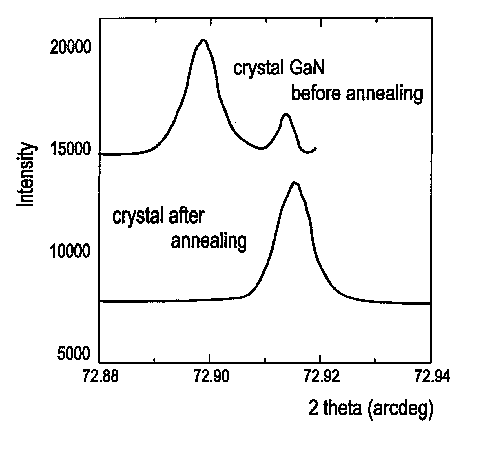
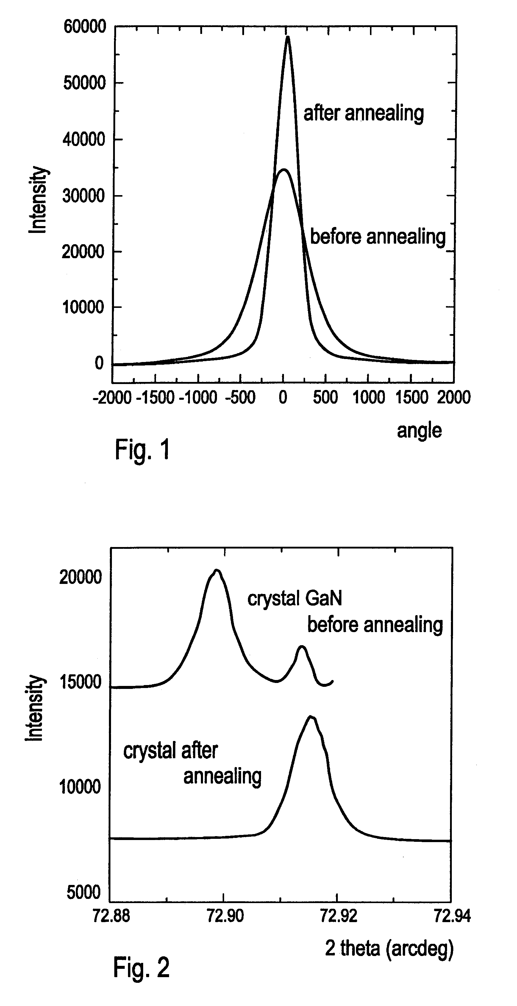
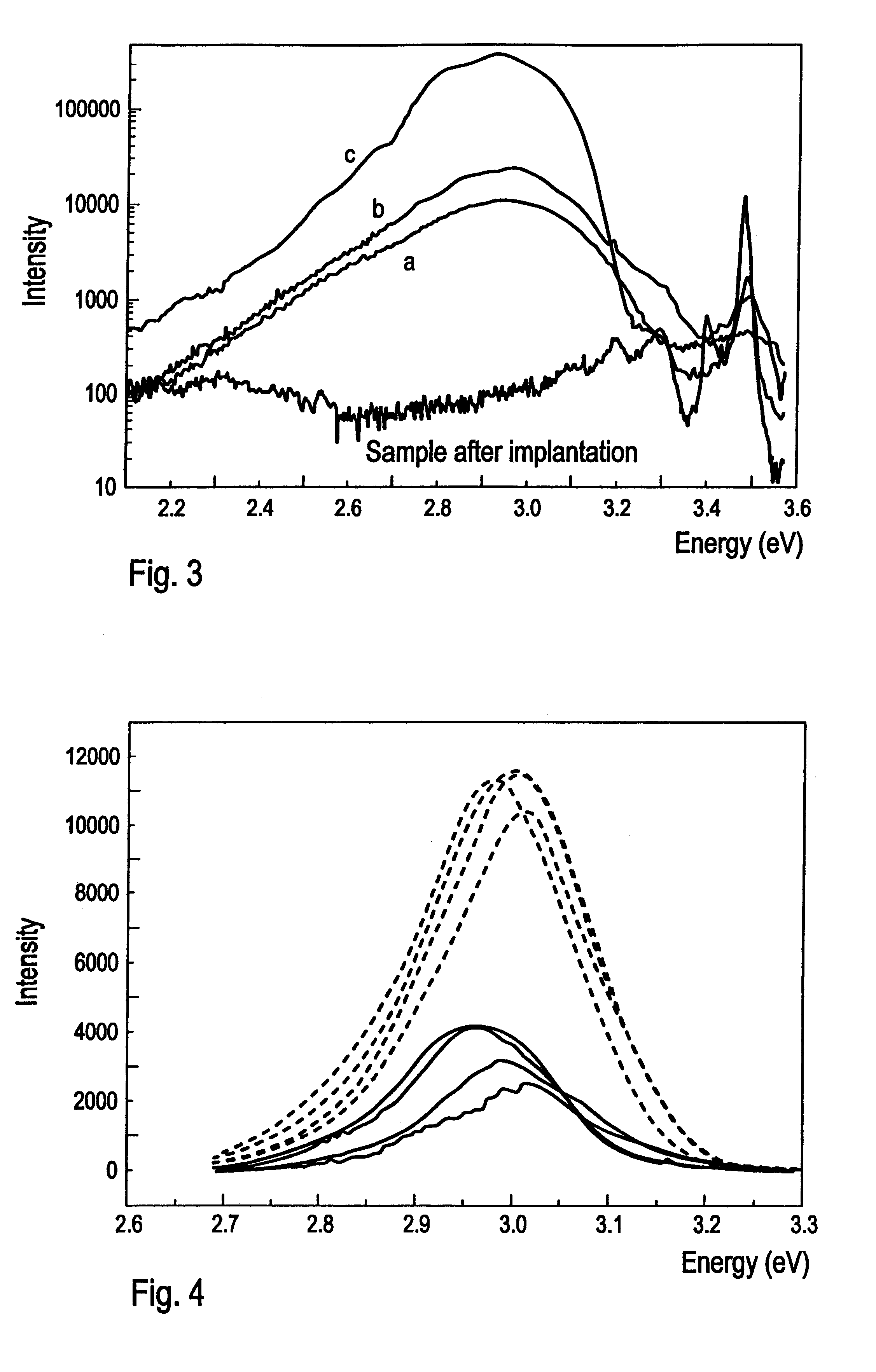
Zn impurity is implanted in room temperature, using the ion energy 200 keV and the total intensity equal to 5.times.10.sup.13 cm.sup.-2. After the implantation, the layer did not show any luminescence for T=80 K and had FWHM=400 arcsec.

The so prepared homoepitaxial structure GaN / GaN is located in quasi-closed graphite container. The conditions of the annealing high pressure process were identical to those in Example 1 except the changes made in the following parameters: duration--1 hour, temperature--1400.degree. C. N.sub.2 a...

example 3

Method of Fabrication of p-type GaN Structures of Improved Structural and Optical Properties by Mg Implantation and High Pressure Diffusion and Autodiffusion

Homoepitaxial GaN structure is prepared as in Example 1. Mg impurity is implanted in room temperature, using the ion energy 200 keV and the total intensity 5.times.10.sup.13 cm.sup.-2. After the implantation, the layer did not show any luminescence for T=80 K and had FWHM=450 arcsec.

Subsequently the so prepared homoepitaxial structure GaN / GaN is located in quasiclosed graphite container The conditions of the process were identical to those in Example 2 except the temperature--1350.degree. C. In the container there was no additional source of Mg.

After extraction of the described GaN structure from high pressure diffusional chamber, the following measurements of undoped GaN structure have been made: Hall effect, electric conductivity, halfwidth of x-ray diffraction peak and photoluminescence at T=80 K.

The layer has the following p...

example 4

Method of Fabrication of p-type GaN Structures of Improved Structural and Optical Properties by Mg Diffusion from Mg-doped Homoepitaxial Layers

Homoepitaxial GaN structure consists of the monocrystalline semiinsulating GaN Mg-doped substrate on which the following layers are deposited by MOCVD method:

buffer layer of undoped GaN of the thickness of 20 nm

Mg-doped GaN layer of the thickness of 1 .mu.m.

undoped GaN layer of the thickness of 1 .mu.m.

protective Si.sub.3 N.sub.4 cap layer of the thickness of 20 nm

The substrate is obtained by high pressure--high temperature growth. The homoepitaxial structure GaN / GaN is located in quasi-closed graphite container together with GaN powder, which consist of 0.03 volume of the entire container. The conditions of the process were identical to those in Example 3. In these conditions during 30 minutes of annealing process Mg impurity diffused from the doped layer to the undoped layer.

After extraction of the described GaN structure from high pressure...


PUM

PropertyMeasurementUnit
pressureaaaaaaaaaa
temperatureaaaaaaaaaa
hole concentrationaaaaaaaaaa

Abstract

The subject of the Invention is the method of fabrication of nitride semiconductor A3B5 such as GaN, AlN, InN or their solid solutions, characterized by p- or n-type conductivity, high intensity of emitted light and high structural quality. The semiconductors obtained by this method are applied in the construction of light emitting devices, light detectors and electric current amplifiers such as for example: highly efficient blue and green light diodes, laser diodes and high power lasers, ultraviolet detectors and high temperature field transistors. The method according to the Invention is characterized by the fact that the homoepitaxial or heteroepitaxial layers of nitride semiconductors A3B5 are deposited on the conductive substrate after the introductory processing or isolating substrate, and after that the so prepared structures are located in high pressure diffusional chamber filled with the one or multi-component gas, compressed to pressure in the range 1000-20000 bar, and annealed in the temperature 1000-1800 ° C. in the prescribed time in the presence of the dopant from the external and / or internal source.

Description

This Invention relates to the method of fabrication nitride semiconductors A.sub.3 B.sup.5 of p- and n-type electric conductivity for manufacturing of optoelectronic devices.OBJECT AND SUMMARY OF THE INVENTIONThe subject of the Invention relates to the method of fabrication of nitride semiconductors A.sub.3 B.sub.5 such as GaN, AIN, InN and their solid solutions, characterized by p- and n-type electric conductivity, low electric resistivity, high intensity of emitted light and high structural quality.The semiconductors obtained by this method are applied in the construction of optoelectronic light emitting devices, light detectors and electric current amplifiers such as e.g.: highly efficient blue and green diodes, laser diodes, high power lasers, ultraviolet detectors and high temperature field effect transistors.The layers of nitrides A.sub.3 B.sub.5 are obtained most frequently by metaloorganic chemical vapor deposition (MOCVD) on sapphire substrates. In this method the metaloorg...

Claims


Application Information

Patent Timeline
Patent Type & Authority Patents(United States)
IPC IPC(8): C30B25/02H01L21/205H01L21/02H01L33/00H01L21/225H01L21/265H01L33/32H01S5/323
CPCC30B25/02C30B29/403C30B29/406H01L21/0237H01L21/02458H01L21/0254H01L21/02576H01L21/02579H01L21/02634H01L33/325
Inventor POROWSKI, SYLWESTERJUN, JANSUSKI, TADEUSZSKIERBISZEWSKI, CZESLAWLESZCZYNSKI, MICHALGRZEGORY, IZABELLATEISSEYRE, HENRYKBARANOWSKI, JACEKLITWIN-STASZEWSKA, ELZBIETA
Owner INST WYSOKICH CISNIEN POLSKIEJ AKADI NAUK
Why Eureka
Try Eureka