Integrated optoelectronic device with an avalanche photodetector and method of making the same using commercial CMOS processes

a technology of optoelectronic devices and avalanche photodetectors, which is applied in the direction of radio frequency controlled devices, instruments, transistors, etc., can solve the problems of communication system performance, difficult to develop integrated solid-state photodetectors, and rendering silicon-based photodetectors made in cmos processes impractical for high-speed data communication systems

Inactive Publication Date: 2002-03-19
LUCENT TECH INC
View PDF9 Cites 21 Cited by
  • Summary
  • Abstract
  • Description
  • Claims
  • Application Information

AI Technical Summary

Benefits of technology

According to one aspect of the present invention, the inventive integrated avalanche photodetector (APD) is capable of being realized in concert with CMOS electronics, and can be fabricated in the same substrate using bulk CMOS-compatible processes. An advantage of such a photodetector is that it is inexpensive to manufacture and avoids the added complexity and parasitic electronic effects associated with packaging silicon-based receiver circuits with detectors made of different or separate materials.
In a currently preferred embodiment, an integrated optoelectronic circuit chip for optical data communication systems includes at least one MOS transistor formed on a portion of a silicon substrate, and an avalanche photodetector (APD) formed on another portion of the silicon substrate. The chip includes a light absorbing region extending from a top surface of the silicon substrate to a depth h and doped to a first conductivity type. The light absorbing region is capable of being ionized by the incident optical signal to form freed charge carriers. A light responsive region is formed in the light absorbing region and extends from the top surface of the silicon substrate to a depth less than h. The light responsive region is doped to a second conductivity type of opposite polarity to the first conductivity type, such that the light absorbing region and light responsive region form a P-N junction at the interface between the light absorbing region and light responsive region so that when the light absorbing region and the light responsive region are reverse biased to near the breakdown voltage, the freed charge carriers in the light absorbing region ionized by the incident optical signal are amplified by avalanche multiplication. The APD further includes a guard ring extending circumferentially along an edge of the light responsive region and configured for preventing premature breakdown of the APD.
(iii) forming a guard ring circumferentially along an edge of the light responsive region for preventing premature breakdown of the photodetector when the light absorbing region and the light responsive region are reverse biased to create avalanche multiplication conditions.

Problems solved by technology

A number of difficulties have been encountered in the development of integrated solid-state photodetectors, i.e. photodetectors that are built or integrated on the same silicon wafer or chip as that of its associated electronic circuitry.
The problems are far more acute in the field of optical data communications because the speed and sensitivity of the photodetectors can significantly affect the performance of the communication systems.
Since the diffusion process is driven by random motion of the carriers, it is a relatively slow transport mechanism, thereby rendering integrated silicon-based photodetectors made in CMOS process impractical for application in high-speed data communication systems.
Another problem with silicon-based integrated photodetectors is that their manufacturing process must be compatible with that of devices such, for example, as PFETs and NFETs which are co-fabricated on the same silicon chip.
For example, one prior art technique produces a photodetector beneath a relatively thick stack of dielectric layers whose combined thickness cannot be controlled to the level required for anti-reflection coatings.
As a result, such photodetectors have low sensitivity or responsivity, i.e. low gain, and their outputs suffer about 3 dB potential variability in sensitivity from the ideal value.
Such additional processing steps, however, undesirably increase the complexity and cost of fabrication.
A problem with these approaches is that there exists large lattice mismatch between the III-V epitaxial layers and the silicon substrate; such a defect degrades the response of such photodetectors.
Although acceptable for monitoring applications, such photodetectors do not meet the stringent requirements of optical data communication systems that operate at data rates of 200 Mbits per second or more.

Method used


Image

  • Integrated optoelectronic device with an avalanche photodetector and method of making the same using commercial CMOS processes
  • Integrated optoelectronic device with an avalanche photodetector and method of making the same using commercial CMOS processes
  • Integrated optoelectronic device with an avalanche photodetector and method of making the same using commercial CMOS processes

Examples


Embodiment Construction

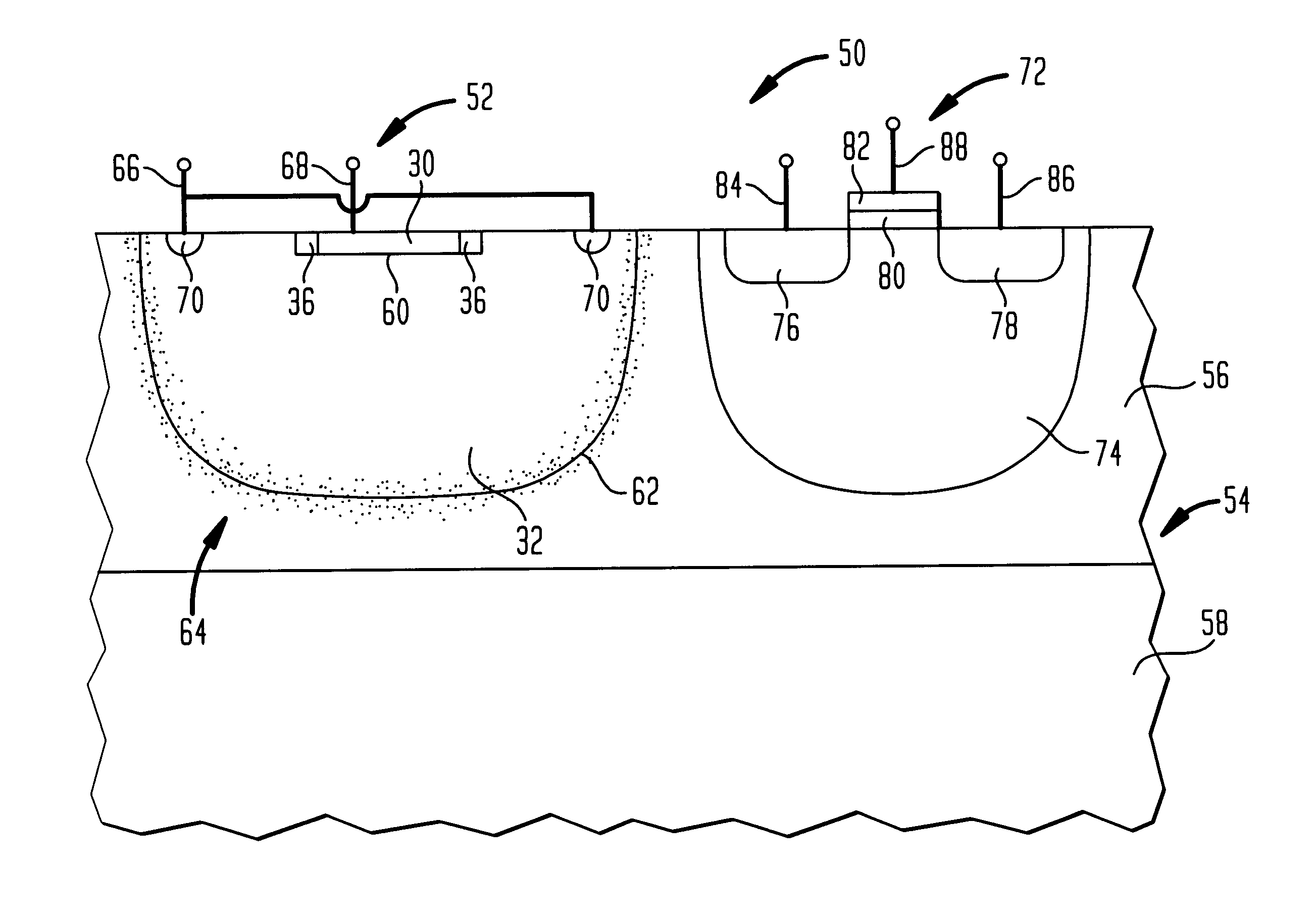
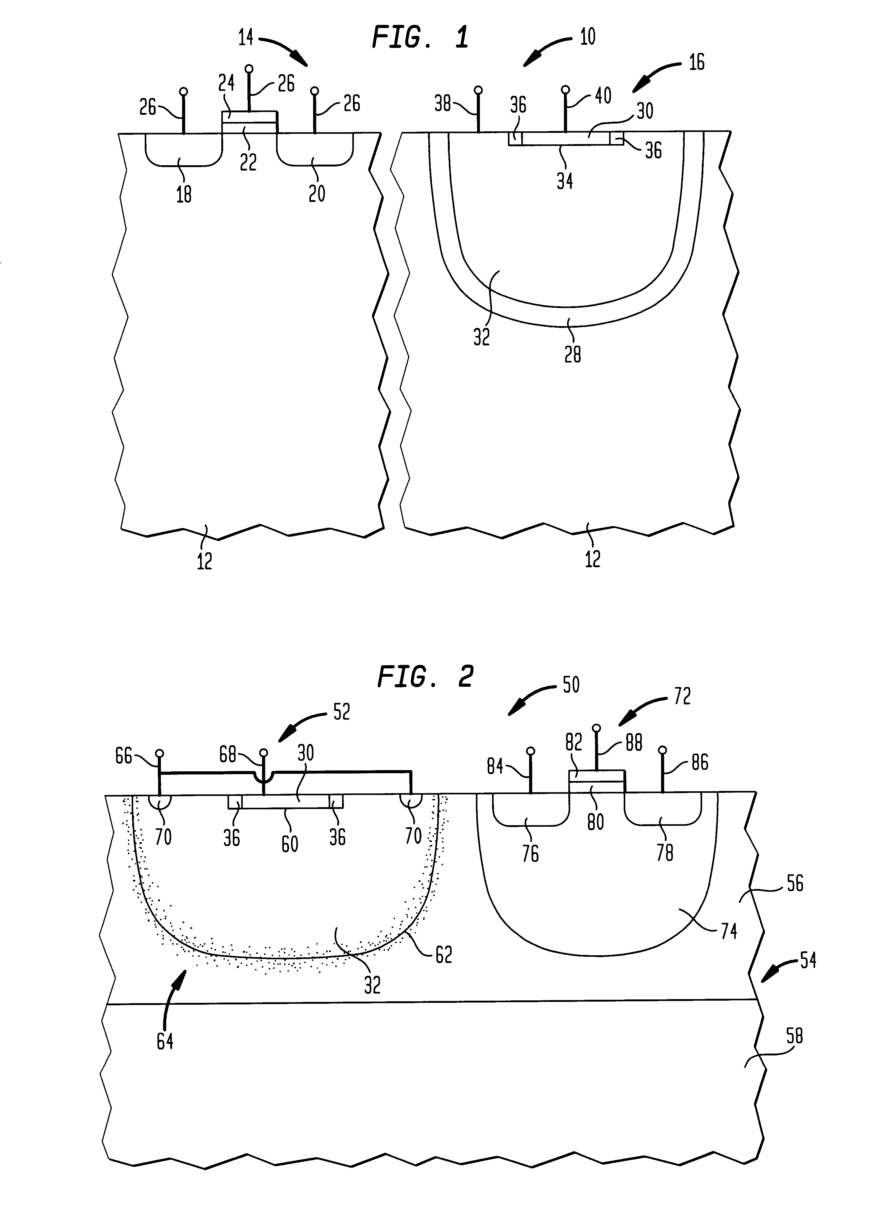
Referring now to the drawings, FIG. 1 illustrates a cross sectional view of an embodiment of an integrated optoelectronic circuit chip 10 of the present invention, and which is manufactured using complementary metal-oxide-silicon (CMOS) processes or other CMOS compatible processes such, for example, as BiCMOS or bipolar processes on a silicon substrate 12. The chip 10 includes at least one metal-oxide semiconductor field effect transistor (MOSFET) 14 and an avalanche photodetector (APD) 16.

As depicted, the MOSFET 14 includes a source region 18 and a drain region 20 diffused or implanted into a region of the substrate 12 that is doped to a conductivity type opposite that of the source and drain regions 18, 20. The MOSFET 14 further includes an oxide layer 22 extending between or spanning the source and drain regions 18, 20, and a metal gate 24 disposed on the oxide layer 22. Electrodes 26 are provided on the source and drain regions 18, 20 and the metal gate 24 for connection with ap...


PUM


Abstract

An integrated optoelectronic circuit chip for optical data communication systems includes a silicon substrate, at least one MOS field effect transistor (MOSFET) formed on a portion of the silicon substrate, and an avalanche photodetector operatively responsive to an incident optical signal and formed on another portion of the substrate. The avalanche photodetector includes a light absorbing region extending from a top surface of the silicon substrate to a depth h and doped to a first conductivity type. The light absorbing region is ionizable by the incident optical signal to form freed charge carriers in the light absorbing region. A light responsive region is formed in the light absorbing region and extends from the top surface of the silicon substrate to a depth of less than h. The light responsive region is doped to a second conductivity type of opposite polarity to the first conductivity type. The light absorbing region and the light responsive region form a P-N junction at the interface therebetween such that when the light absorbing and light responsive regions are appropriately reverse biased, the freed charge carriers in the light absorbing region are amplified by avalanche multiplication.

Description

1. Field of the InventionThe present invention relates to optoelectronic devices and, in particular, to a silicon-based integrated optoelectronic circuit chip having an avalanche photodetector and a method of making the chip using CMOS compatible processes.2. Description of the Related ArtA number of difficulties have been encountered in the development of integrated solid-state photodetectors, i.e. photodetectors that are built or integrated on the same silicon wafer or chip as that of its associated electronic circuitry. Resolution of the problems requires the developer to optimize myriad parameters involving the properties of optical communication systems (e.g. operating wavelengths), fundamental optical properties of silicon (e.g. the band gap energy of Si and thus its wavelength absorption), and properties of other co-fabricated devices (e.g. P-type field effect transistor (PFET) or N-type field effect transistor (NFET)) which are to be simultaneously fabricated with the photod...

Claims


Application Information

Patent Timeline
Patent Type & Authority Patents(United States)
IPC IPC(8): G11C13/00H01L21/00H01L29/66H01L31/112H01L31/0328H01L31/06H01L29/80H01L31/101H01L31/102H01L31/0264H01L31/072H01L31/109H01L31/107
CPCH01L31/107
Inventor WOODWARD, TED KIRK
Owner LUCENT TECH INC
Why Eureka
Try Eureka