Technology for thermodynamically stable contacts for binary wide band gap semiconductors

a technology of wide band gap semiconductors and contacts, applied in semiconductor/solid-state device manufacturing, basic electric elements, electric apparatus, etc., can solve the problems of limited ability to use stable contact design, limited applicability of phase diagrams, and added complexity of ternary reactions

Inactive Publication Date: 2002-06-25
RAMOT UNIV AUTHORITY FOR APPLIED RES & INDAL DEVMENT +1
View PDF1 Cites 38 Cited by
  • Summary
  • Abstract
  • Description
  • Claims
  • Application Information

AI Technical Summary

Problems solved by technology

On the other hand, for compound semiconductors, the search for contacting solutions is still widely pursued, while the primary obstacle is the added complexity of ternary reactions.
Despite the rapid built-up of ternary phase diagram knowledge base during the last decade, the ability to use it for stable contact design is limited.
For example, the applicability of phase diagrams is limited to closed thermodynamic systems.
Maintaining a closed system is difficult in compounds such as Group III arsenides and nitrides since one of the elements is volatile.
The complexity is also manifested in the reaction kinetics.
As a result, in systems, such as silicon carbides, the obtained contact is typically composed of a mixture of phases, which is of limited use in the sub-micron regime and can affect the electrical characteristics of the contact.
The use of devices produced from such semiconductors is generally limited to operation at ambient or, at most, moderately elevated temperatures and in non-corrosive, inert atmospheres.
The temperature limitation is a consequence of the small band gap of these materials,(1-1.5 eV) which leads to large leakage currents and device failure at elevated temperatures.
In addition, rapid diffusion of dopants and / or impurity species in the host material can occur, which in turn can substantially alter the character of the fabricated semiconductor device.
The limitation to relatively inert environments results from the high chemical reactivity of moderate band gap semiconductors (including silicon) to many corrosive environments, which also can alter the character of the fabricated device.
Such devices are also limited as to power level, frequency, and radiation tolerance by the materials used therein.
In other applications, these limitations have prevented the use of silicon for integrated circuit technology.
For example, in many spacecraft and aircraft applications, elevated temperatures are encountered, and it is not always possible to insure that adequate cooling will be provided.
In high power applications, device temperatures can rise to levels, which degrade or destroy the device solely through internal heating.
Silicon's inability to withstand high temperatures limits the amount of power, which can be generated or controlled by silicon electronics.
In addition, internal thermal transients in devices otherwise operating at ambient temperature can rapidly destroy the operability of the device unless extensive cooling is provided.
Such cooling requires that the device be larger in size than might otherwise be necessary, in part defeating the purpose of the integrated circuit technology.
There has therefore been an ongoing, but as yet not fully successful, search over a period of twenty years to identify and develop a semiconductor technology based in other materials.
The metal-semiconductor contact is a crucial building block in the making of any electronic device based on these semiconductors that is intended to be operated at high temperatures.
However, at elevated temperatures the metal semiconductor junction appears to become unstable.
Attempts to achieve limited stability have been made using complex contacts composed of several layers, one of which is usually used as a diffusion barrier.
However, this contact has a very limited lifetime at high temperatures (>300.degree. C.) at which diffusion eventually occurs and the undesirable reaction takes place.
However, this type of contact may only serve as an ohmic contact, since it does not provide an "in-situ" formation of a new interface such as in the case of Si silicidation, which is required for high quality and reproducible Schottky barriers.
However, this contact does not provide a solution for the carbon product due to the very small quantity of Ti.
Moreover, the preparation of the alloy is a complicated process as compared to the more common layer-by-layer deposition.

Method used


Image

  • Technology for thermodynamically stable contacts for binary wide band gap semiconductors
  • Technology for thermodynamically stable contacts for binary wide band gap semiconductors

Examples


Embodiment Construction

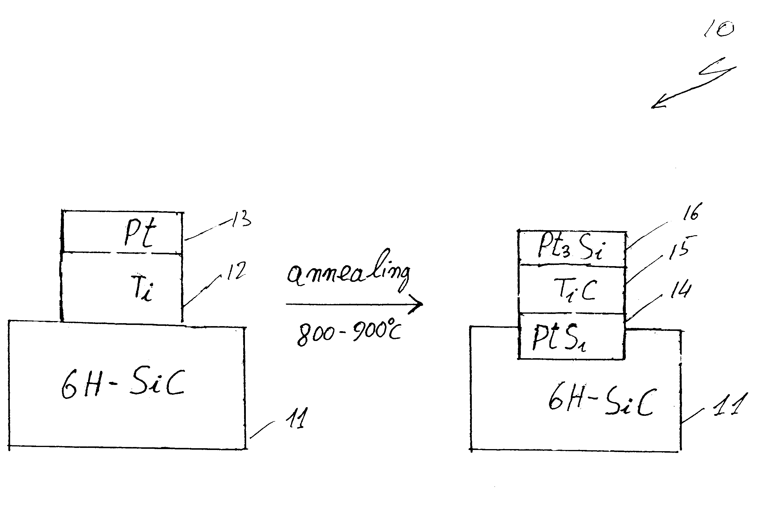
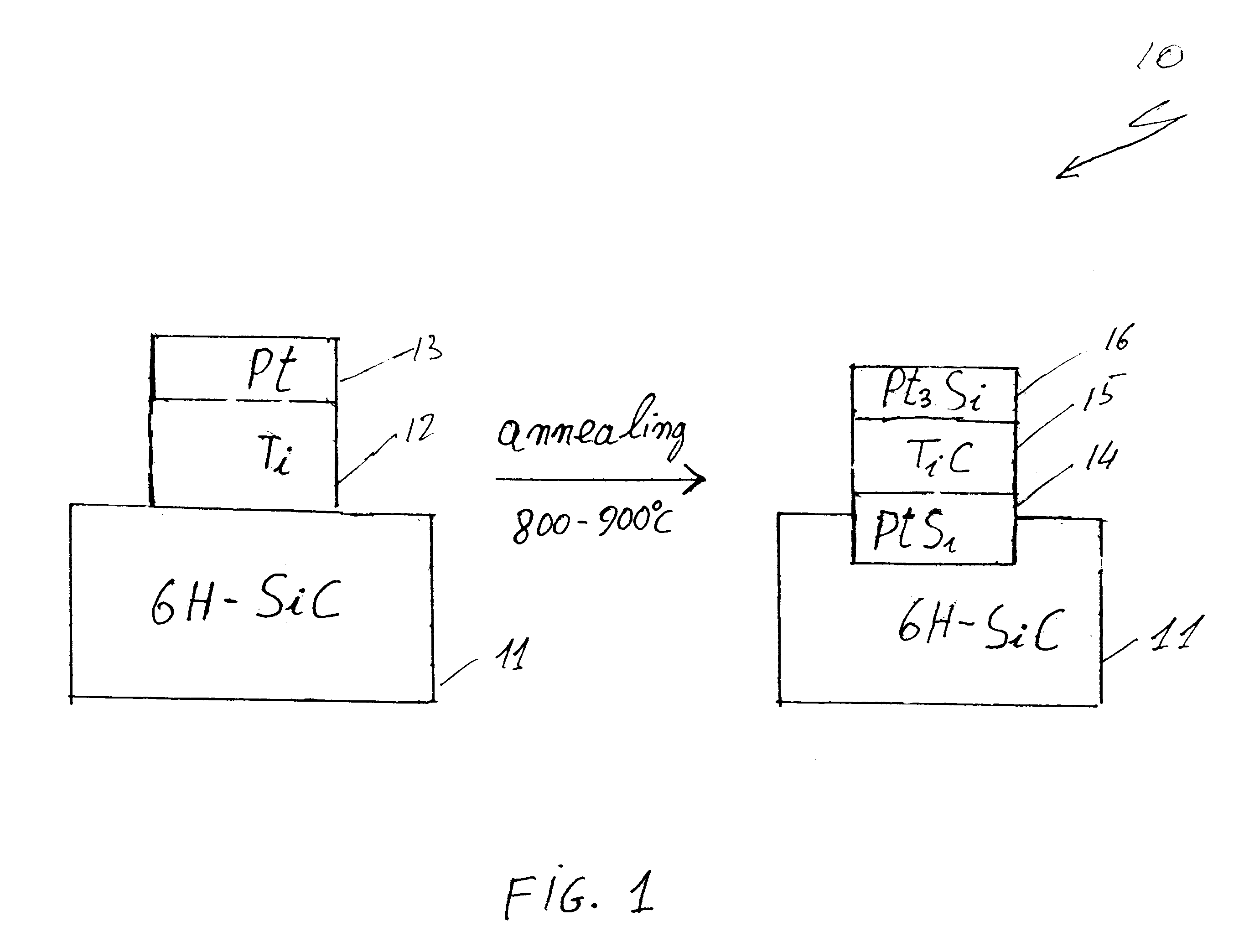
Preparation of Ti.backslash.Pt contact for 6H-SiC.

Two metallic layers were deposited sequentially without breaking the vacuum, using e-beam thermal deposition under vacuum of 1.multidot.10.sup.-8 Torr onto two 6H-SiC substrate samples. The substrates (11 in FIG. 1) were neither cooled nor heated externally.

As shown schematically in FIG. 1, the first layer 12 consisted of Ti and was 16-nm-thick. The second layer 13 consisted of Pt and was 8-nm-thick. One sample was kept as a reference while the other was heat-treated in an evacuated tube furnace under vacuum of 1.multidot.10.sup.-7 Torr for an hour at 800.degree. C. and for another hour at 900.degree. C.

Then the samples were depth-profiled using x-ray photoelectron spectroscopy (XPS) in conjunction with ion sputtering. The craters, formed by the sputtering, were analyzed using crater edge scanning Auger microscopy. The XPS results were used for chemical identification of the phases, while the crater edge profiling was used to obtain ...


PUM

PropertyMeasurementUnit
pressureaaaaaaaaaa
temperatureaaaaaaaaaa
temperaturesaaaaaaaaaa

Abstract

A thermodynamically stable metallic contact for binary oxide-, nitride-, carbide or phosphide-semiconductors and a method of its preparation, the contact is formed in a high temperature reaction in vacuum of a metal bi-layer with the binary semiconductor substrate. With a proper choice of the two metallic layers, each metal forms a single phase with only one of binary semiconductor elements. The resulting phases form distinct layers in a thermodynamically stable sequence.

Description

BACKGROUND OF THE, INVENTIONThis invention relates to a process for the preparation of thermodynamically stable metallic contacts for binary oxide-, nitride-, carbide- or phosphide-semiconductors. The product of this invention, the metal-semiconductor contact, is a crucial building block in the making of any electronic device based on these semiconductors that is intended to be operated at high temperatures. In particular, this method is useful for making metal contacts to group III nitrides and to silicon carbides.Metal contacts to modem silicon devices typically incorporate a transition-metal / silicide contacting layer. The formation of transition-metal silicides and their characteristics have been exhaustively investigated, and their current manufacturing technology provides a satisfactory solution for contacting silicon devices. On the other hand, for compound semiconductors, the search for contacting solutions is still widely pursued, while the primary obstacle is the added comp...

Claims


Application Information

Patent Timeline
Patent Type & Authority Patents(United States)
IPC IPC(8): H01L21/02H01L29/40H01L29/45H01L21/04H01L29/47H01L21/285H01L29/02H01L29/20H01L29/24
CPCH01L21/048H01L21/0485H01L21/0495H01L21/28575H01L21/28581H01L29/475H01L29/45H01L29/452H01L29/456H01L29/47H01L29/20H01L29/1608
Inventor SHALISH, ILANSHAPIRA, YORAMEIZENBERG, MOSHE
Owner RAMOT UNIV AUTHORITY FOR APPLIED RES & INDAL DEVMENT
Why Eureka
Try Eureka