

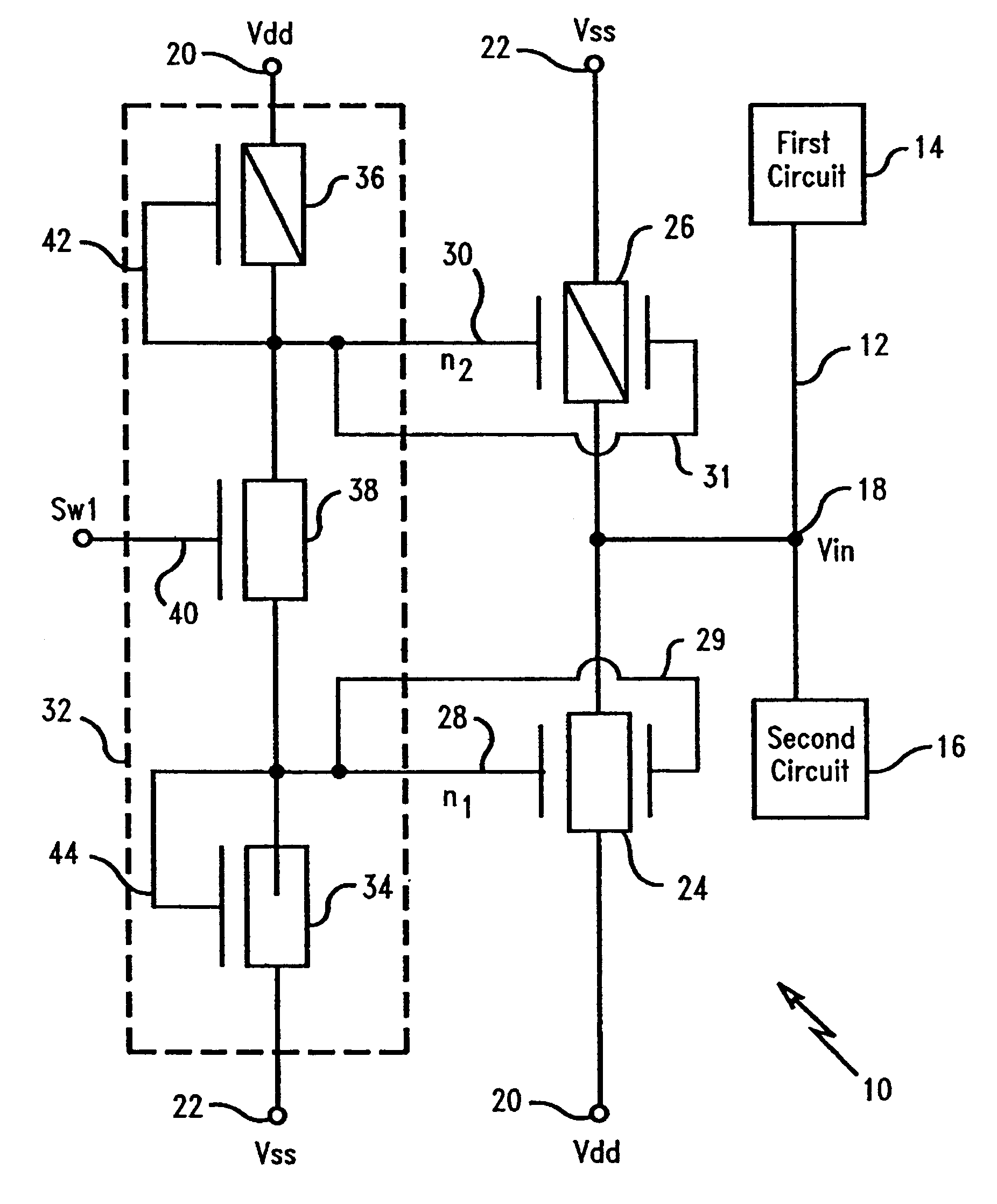
Double-gate low power SOI active clamp network for single power supply and multiple power supply applications
a low-power soi active clamping and single-gate technology, applied in the direction of pulse automatic control, pulse technique, semiconductor devices, etc., can solve the problems of inability to effectively meet the requirements of the highest-performance applications of passive clamping circuits, inability to switch input voltage generally takes a finite amount of time, and degrade the circuit's performance, so as to achieve the effect of improving performan
- Summary
- Abstract
- Description
- Claims
- Application Information
AI Technical Summary
Benefits of technology
Problems solved by technology
Method used
Image

Examples
first embodiment
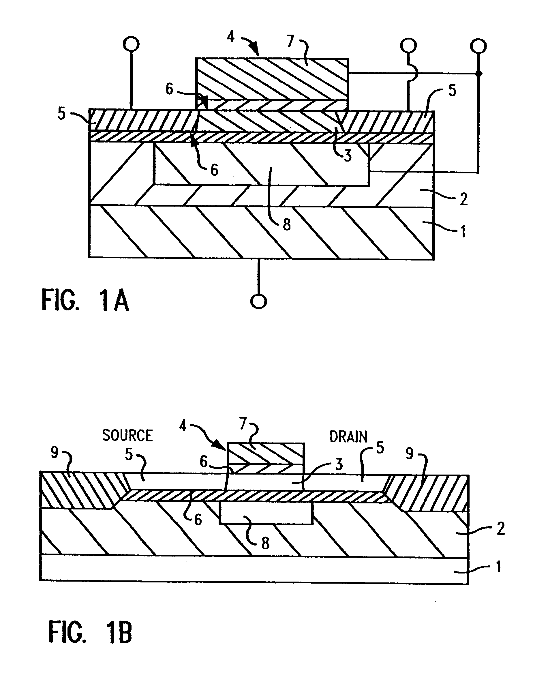
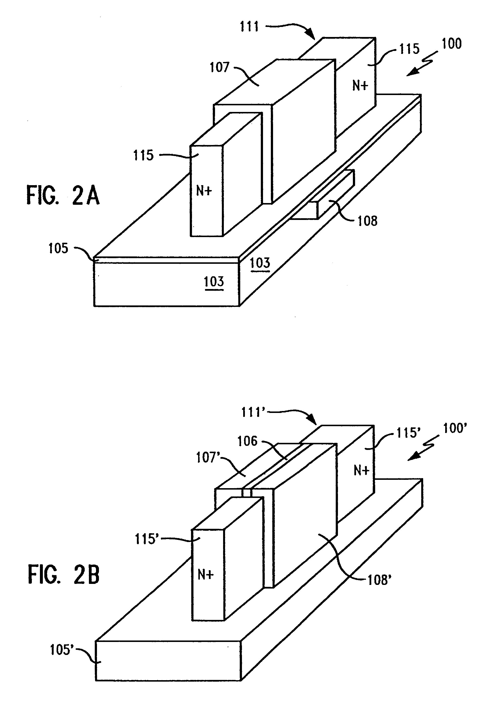
In the double-gated FINFET transistors, as shown in FIG. 2A, the double-gated FINFET 100 may be provided by first forming a bottom gate 108 in a buried oxide (BOX) region 103 by known techniques for formation of a bottom gate SOI device. For example, the bottom gate 108 of the present double-gated FINFET 100 clamping network may be formed by providing an insulator layer on a silicon wafer, etching a region in the insulator layer, deposition of a gate material thereover the wafer followed by providing a second insulator film thereover the film, and subsequently bonding with a second wafer of silicon. The bottom gate 108 may comprise a conductive material including metal, polysilicon or any other conductive material known and used in the art. The top gate 107 of the instant FINFET transistors may then be formed by standard FINFET development procedures. In so doing, a thin rectangular region 111 of silicon, or silicon island, is formed on the insulator layer 105 after an etch step. A ...
second embodiment
In the double-gated FINFET transistors, as shown in FIG. 2B, a double-gated FINFET 100' may be provided by splitting the FINFET formed by standard FINFET development procedures as described above in relation to the formation of the top gate 107 of FINFET 100. In so doing, FINFET 100' may be formed using SOI technology. A thin rectangular region 111' of silicon, or silicon island, is formed on the insulator layer 105', after an etch step, followed by formation of a gate dielectric material around a middle portion of the silicon island 111' to form a gate structure over the gate insulator. Source and drain regions 115' are implanted. A portion of the gate dielectric material at the middle of the gate structure is removed by etching and then an insulator layer 106, such as an oxide, is provided in such removed portion of the gate structure, thereby splitting the gate structure into a first, front gate 107' and a second, back gate 108'.
In accordance with the invention, the first gate (o...
PUM
 Abstract
Description
Claims
Application Information