Organic electroluminescent device

an electroluminescent device and organic technology, applied in the direction of discharge tube luminescnet screen, thermoelectric device, discharge tube/lamp details, etc., can solve the problems of significant acceleration of the degradation of organic thin films, sensitivity to electrodes, and the organic materials of which the organic layers are formed. , to achieve the effect of long life, high efficiency and low cos

Inactive Publication Date: 2002-09-03
TDK CORPARATION
View PDF25 Cites 96 Cited by
  • Summary
  • Abstract
  • Description
  • Claims
  • Application Information

AI Technical Summary

Benefits of technology

An object of the present invention is to provide an organic EL device capable of utilizing the advanta

Problems solved by technology

Reliability is a common problem to be solved for these organic EL devices.
However, the organic materials of which the organic layers are formed are vulnerable during manufacture and have less affinity to the electrodes.
Another problem is raised by the significantly accelerated degradation of organic thin films as compared with light emitting diodes (LED) and laser diodes (LD).
Although these devices are effectively and widely utilized, their size is so small that it is not only difficult, but also uneconomical to apply the LEDs to large area displays.
The ZnS system, however, suffers from serious practical drawbacks including the lack of reliability.
On practical use, these organic materials have the problems that they lack reliability like ZnS, and joining layers of these materials to current-injecting electrode layers is difficult.
The technique of depositing organic materials t

Method used


Image

  • Organic electroluminescent device
  • Organic electroluminescent device
  • Organic electroluminescent device

Examples


example 1

A substrate of (7059) glass by Corning Glass Works was scrubbed using a neutral detergent.

By RF magnetron sputtering from a target of ITO oxide, a hole injecting electrode layer of ITO having a thickness of 200 nm was formed on the substrate at a temperature of 250.degree. C.

After its ITO electrode-bearing surface was cleaned with UV / 03, the substrate was secured by a holder in a sputtering chamber, which was evacuated to a vacuum of 1.times.10.sup.-4 Pa or lower.

Using a target of SiO.sub.2, an inorganic insulative hole injecting layer was deposited to a thickness of 2 nm. The sputtering gas used was a mixture of 100 sccm of argon and 10 sccm of oxygen (O.sub.2). Sputtering conditions included a substrate temperature of 25.degree. C., a deposition rate of 1 nm / min, an operating pressure of 0.5 Pa, and an input power of 5 W / cm.sup.2 The hole injecting layer as deposited had a composition of SiO.sub.1.7.

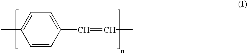
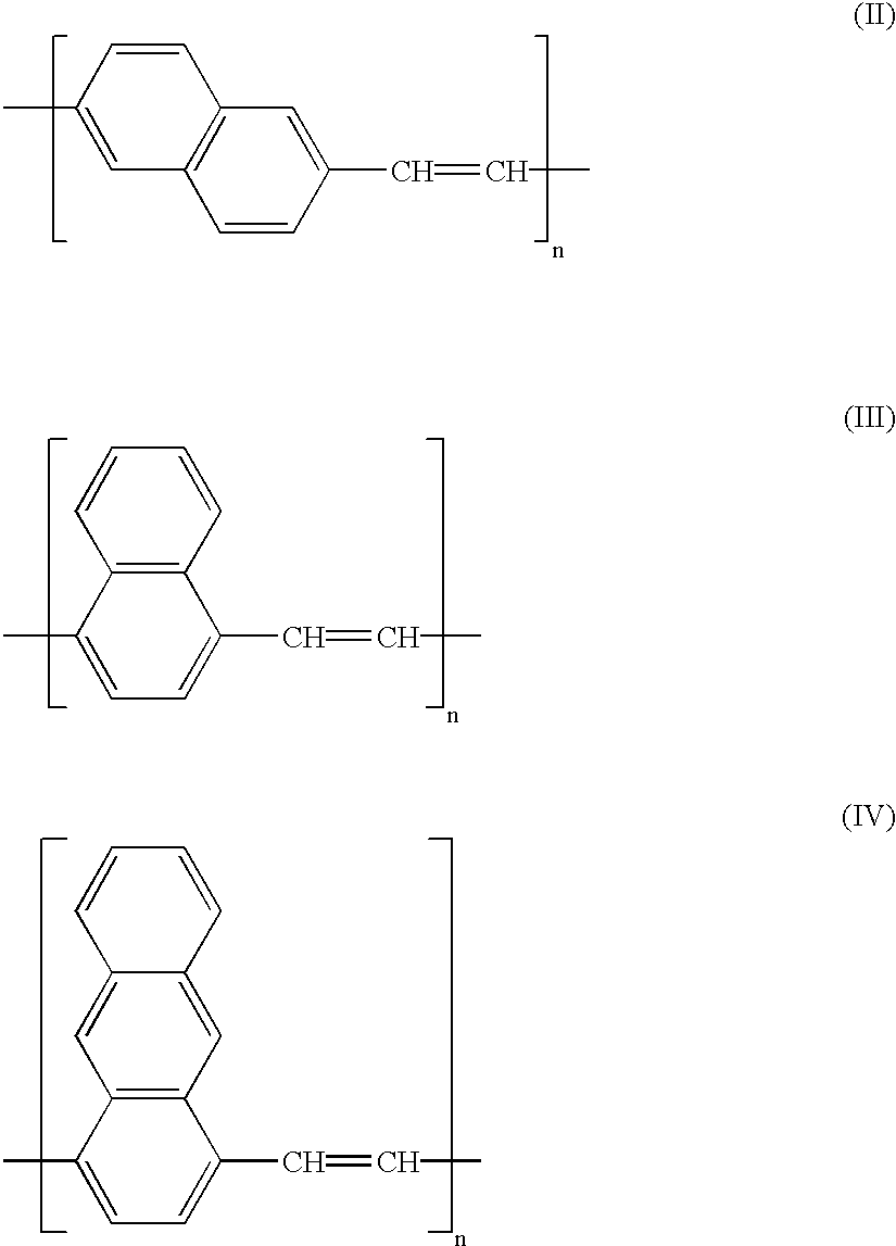
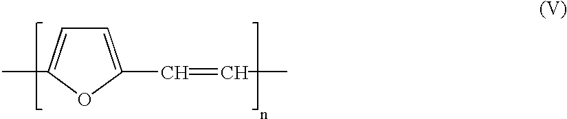
A methanol solution of a PPV precursor having a concentration of 1 g of polymer pe...

example 2

In Example 1, the PPV film was formed directly on the ITO electrode without interleaving the inorganic insulative hole injecting layer.

With the vacuum kept, the substrate was transferred to a sputtering chamber. Using a mixture of potassium oxide (K.sub.2 O, electron affinity 2.0 eV) and 5 mol % of silicon oxide (SiO.sub.2) as the target, an inorganic electron injecting layer was deposited to a thickness of 1 nm. Sputtering conditions included a substrate temperature of 25.degree. C., a 1:1 mixture of sputtering gas Ar and oxygen (O.sub.2), a deposition rate of 1 nm / min, an operating pressure of 0.5 Pa, and an input power of 5 W / cm.sup.2.

Thereafter, as in Example 1, the electron injecting layer and auxiliary electrode were formed, obtaining an organic EL device.

The organic EL device was examined as in Example 1, finding equivalent results to Example 1.

example 3

An organic EL device was fabricated as in Example 1 except that the inorganic insulative electron injecting layer of Example 2 was formed after the formation of the PPV film.

The organic EL device was examined as in Example 1, finding equivalent results to Example 1.


PUM


Abstract

An organic EL device has a hole injecting electrode (2), an electron injecting electrode (6), an organic layer participating in a light emitting function disposed between the electrodes. The organic layer includes a light emitting layer (4) comprising a conjugated polymer. The device further includes an inorganic insulative hole injecting layer (3) or an inorganic insulative electron injecting layer (5). The device can take advantage of both organic and inorganic materials, and has an improved efficiency, an extended effective life, and a low cost.

Description

This invention relates to an organic electroluminescent (EL) device and more particularly, to an inorganic / organic junction structure suitable for use in a device of the type wherein an electric field is applied to a thin film of an organic compound to emit light.BACKGROUND OF THE INVENTIONActive research works have been made on organic EL devices for use as displays because EL devices can be formed on a large area of glass. In general, organic EL devices have a basic configuration including a glass substrate, a transparent electrode of tin-doped indium oxide (ITO) etc., a hole transporting layer of an organic amine compound, a light emitting layer of an organic fluorescent material exhibiting electronic conductivity and intense light emission such as an aluminum quinolinol complex (Alq3), and an electrode of a metal having a low work function such as MgAg, wherein the layers are stacked on the substrate in the described order.The device configurations which have been reported thus ...

Claims


Application Information

Patent Timeline
IPC IPC(8): H01L51/52H01L51/50H05B33/22H05B33/12H05B33/14
CPCH01L51/5088H01L51/5092H05B33/22H10K50/171H10K50/17
Inventor ARAI, MICHIOONITSUKA, OSAMU
Owner TDK CORPARATION
Why Eureka
Try Eureka