Semiconductor integrated circuit device and method of manufacturing the same, and cell size calculation method for DRAM memory cells

a technology of integrated circuits and semiconductors, which is applied in the direction of semiconductor devices, electrical devices, transistors, etc., can solve the problems of large increase of the total process steps, difficult to tighten the wiring pitch in the metal wiring layer, and increase the general chip cos

Inactive Publication Date: 2002-10-01
RENESAS ELECTRONICS CORP
View PDF5 Cites 37 Cited by
  • Summary
  • Abstract
  • Description
  • Claims
  • Application Information

AI Technical Summary

Problems solved by technology

In this case, a large step height, however, occurs between the memory array section and the other peripheral circuit section, which makes it difficult to tight the wiring pitch in the metal wiring layers.
This leads to a large increase of the number of the total process steps, resulting in boosting the general chip cost.
As described above, since the chip size of the SRAM cannot help enlarging drastically in accordance with its large capacity development, which makes it hard extremely to hybridize 4 M (mega) or more SRAMs with logic circuits.

Method used


Image

  • Semiconductor integrated circuit device and method of manufacturing the same, and cell size calculation method for DRAM memory cells
  • Semiconductor integrated circuit device and method of manufacturing the same, and cell size calculation method for DRAM memory cells
  • Semiconductor integrated circuit device and method of manufacturing the same, and cell size calculation method for DRAM memory cells

Examples


embodiment 1

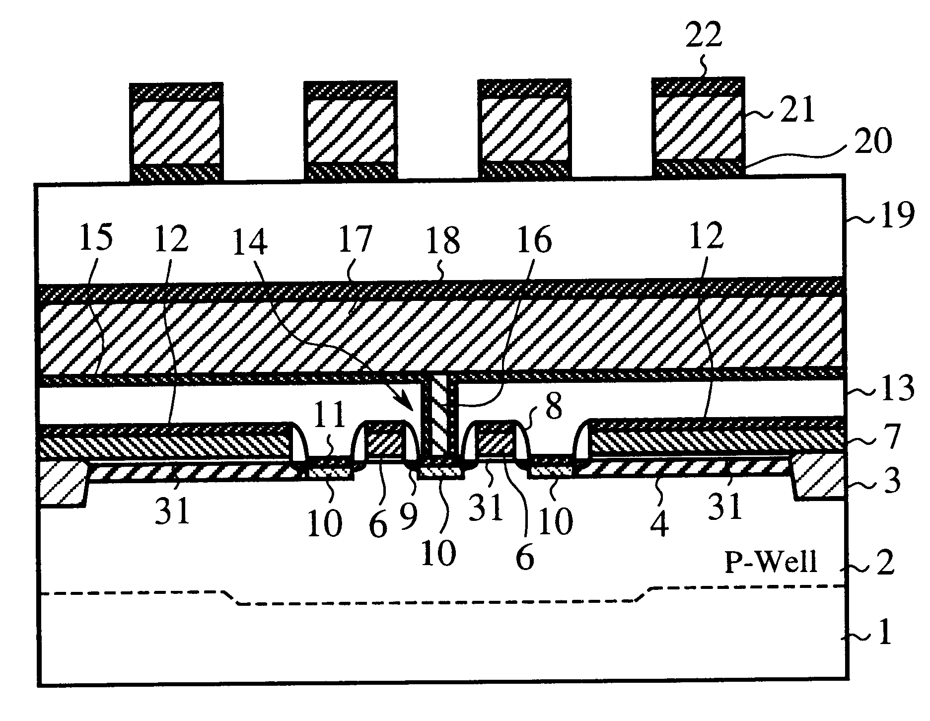
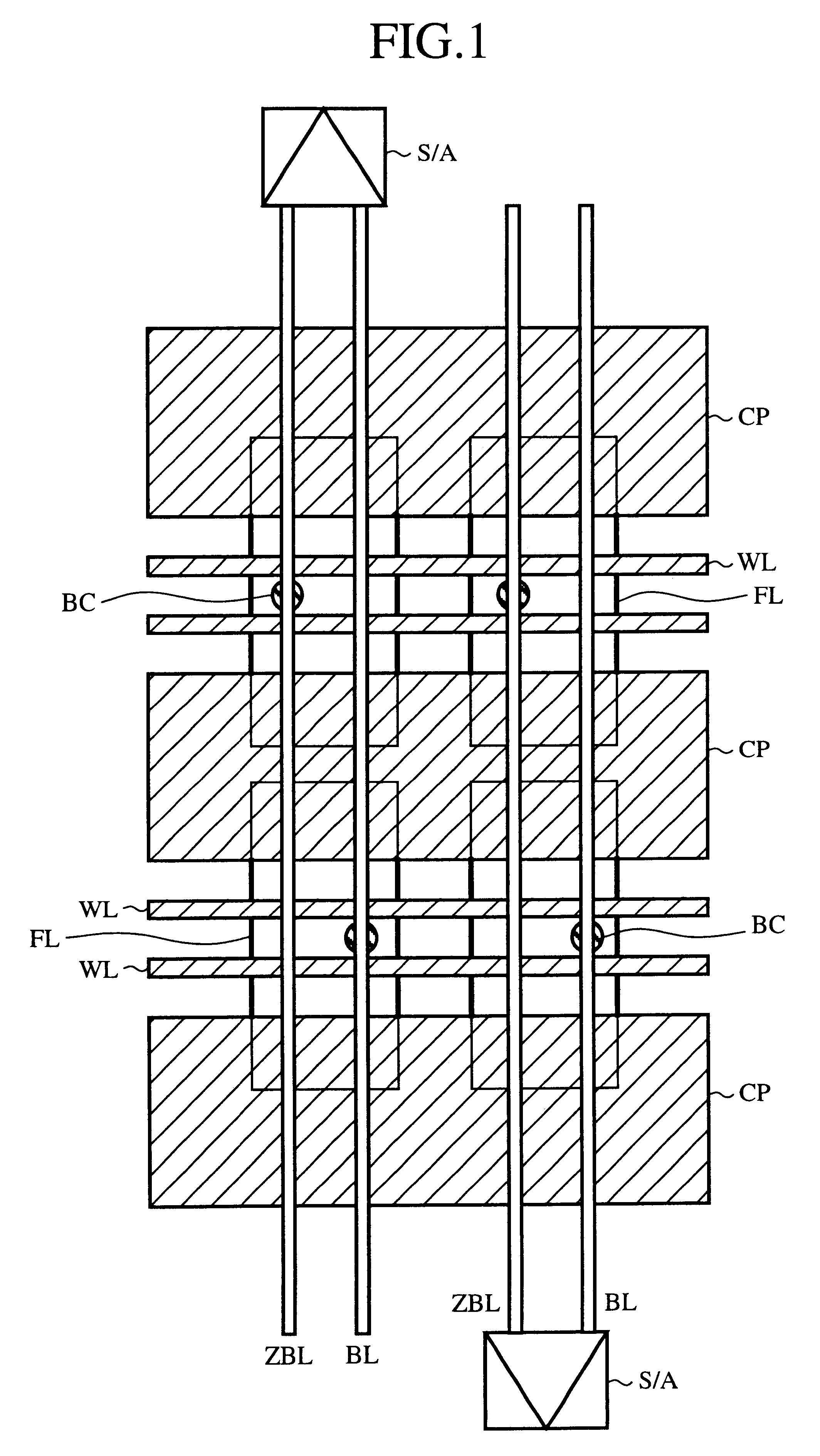
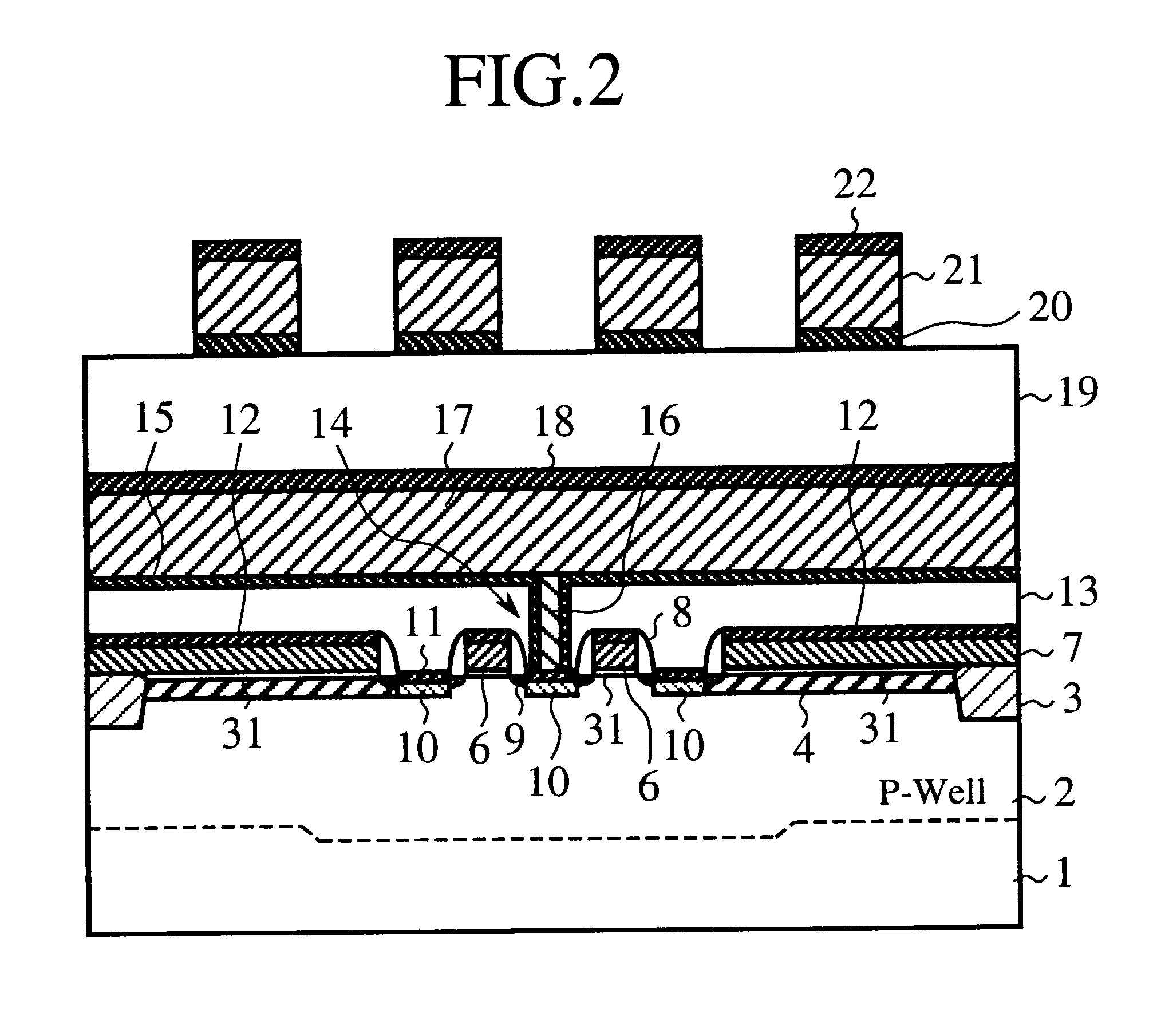
FIG. 1 is a layout diagram showing schematically the configuration of a memory cell array in a semiconductor integrated circuit device in accordance with the present invention, and FIG. 2 is a sectional schematic illustration taken along an arbitrary longitudinal line passing a bit line contact BC of FIG. 1.

In FIGS. 1 and 2, reference symbol BC denotes a bit line contact; WL denotes a word line; BL denotes a non-inversion bit line; ZBL denotes an inversion bit line; CP denotes a cell plate electrode; and S / A denotes a sense amplifier. Reference numeral 1 designates a semiconductor substrate such as silicon; 2 designates a p-type well (including the channel-cut under the isolation region); 3 designates a device isolation region; 4 designates a n-type impurity region for a planar capacitor; 31 designates a gate oxide and a capacitor dielectric; 6 designates a gate electrode; 7 designates a cell plate electrode CP for the planar capacitor; 8 designates a insulating side wall; 9 designa...

embodiment 2

FIG. 10 is a schematic cross section of a semiconductor integrated circuit device in accordance with an embodiment 2 of the present invention. In FIG. 10, reference numeral 40 designates a highly doped impurity region for increasing a coupling capacitance. The same other numerals above designate the same components or corresponding parts and their explanation will be omitted herein for brevity, which is similar in the following.

In the semiconductor integrated circuit device of the embodiment 2, there is a feature in that in the memory cell structure of the embodiment 1, the p+ highly doped impurity region 40 for increasing the coupling capacitance is provided under an impurity region 4 for a planer capacitor. This achieves a memory cell having a Hi-C structure, what is called, and enlarges the capacitance of the node which stores data so as to prevent the data destruction within the memory cell due to soft errors.

Next, a method of manufacturing a semiconductor integrated circuit dev...

embodiment 3

FIG. 12 illustrates a schematic cross section of a semiconductor integrated circuit device in accordance with an embodiment 3 of the present invention, which illustrates the sectional structure of a PDR memory cell. In FIG. 12, reference numeral 31 designates a gate oxide for a MOS transistor; and 31a designates a capacitor dielectric for a signal charge storage capacitor. Note that other components are the same as the embodiment 1.

The semiconductor integrated circuit device of the embodiment 3 has the following feature: In the memory cell structure, the thickness of the capacitor dielectric 31a for the signal charge storage capacitor is formed thinner than that of the gate oxide 31 for the MOS transistor; thus the area of the capacitor may be reduced and the storing amount of the charge may be enhanced.

Next, a method of manufacturing a semiconductor integrated circuit device in accordance with the embodiment 3 will be described with reference to the sectional process flow diagram o...


PUM


Abstract

There is provided a semiconductor integrated circuit device comprising: a field placement creating a field pattern in an array form by closest packing on a first conductance-type semiconductor substrate, the field pattern including a plurality of memory cells which define an active area and a device isolation region of a field effect transistor, and which are arranged in a predetermined pitch in the longitudinal and transverse directions, respectively, each memory cell having a pattern of a certain length-to-width size; a cell plate placement providing a capacitor structure between a second conductance-type diffusion region formed by an impurity implant to the active area and a cell plate electrode formed so as to cover part of the active area with a predetermined cell plate pattern through a capacitor dielectric, the cell plate pattern extending in the transverse direction with a certain length size; and a word line placement in which a word line pattern is arranged in the transverse direction of a vacant zone of the active area in which the cell plate electrode is not formed and serves as a gate electrode of the field effect transistor on the active area, the word line pattern being formed through a gate oxide at a predetermined interval, wherein the layout of a cell array of the memory cells is provided by a closest packing cell configuration.

Description

1. Field of the InventionThe present invention relates to a semiconductor integrated circuit device such as a system LSI incorporating DRAMs, a method of manufacturing the same, and a cell size calculation method for DRAM memory cells.2. Description of the Prior ArtIn recent years, a DRAM mixing or hybrid system LSI which integrates a logic such as processor, ASIC, or the like, and a large-scale DRAM on a common semiconductor substrate has been applied for many purposes. In such a system LSI, an internal data bus of multiple bits, e.g. 128-512 bits, makes an interconnection between the logic and the DRAM, thus achieving a data transmission speed which is higher by one to two orders, as compared to a case that a commercially available DRAM and a logic each having a small number of terminals are connected with each other on a common printed circuit board.In addition, with respect to the logic, the number of external input pins may be reduced as compared to a system configuration which...

Claims


Application Information

Patent Timeline
Patent Type & Authority Patents(United States)
IPC IPC(8): H01L27/108H01L27/02H01L21/8242
CPCH01L27/10805H01L27/0207H10B12/30
Inventor MORIHARA, TOSHINORISHIMANO, HIROKIARIMOTO, KAZUTAMI
Owner RENESAS ELECTRONICS CORP
Why Eureka
Try Eureka