

Method of forming microcrystalline silicon film, method of fabricating photovoltaic cell using said method, and photovoltaic device fabricated thereby
a microcrystalline silicon and film technology, applied in the field of microcrystalline silicon film forming method and the method of fabricating photovoltaic devices, can solve the problems of difficult to enhance throughput upon mass production, difficult to reduce process cost, and the quality of thin film formed tends to be more rapidly deteriorated
- Summary
- Abstract
- Description
- Claims
- Application Information
AI Technical Summary
Benefits of technology
Problems solved by technology
Method used
Image

Examples
example 1-1
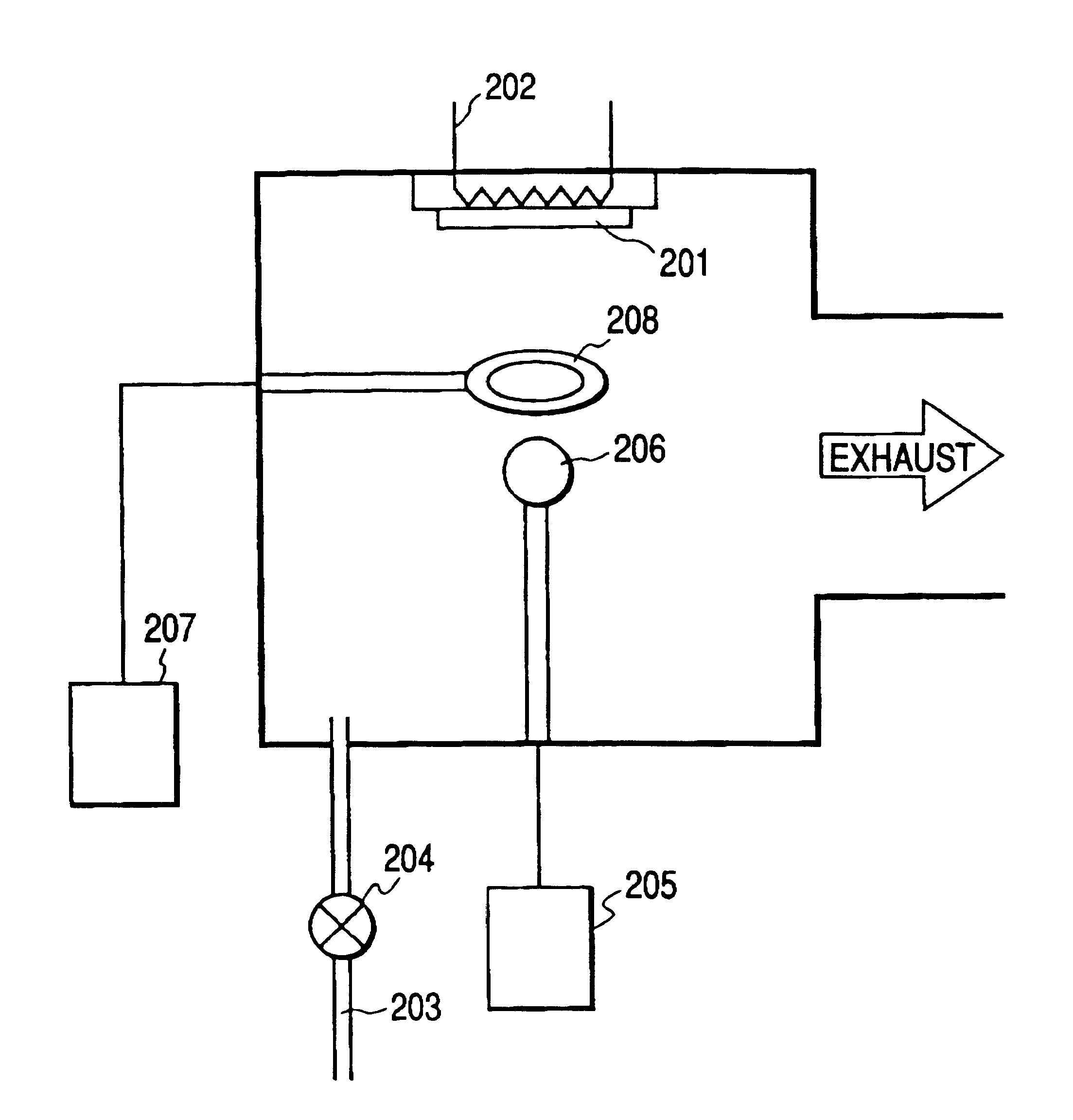
A microcrystalline silicon film having a thickness of about 1 .mu.m was deposited on a 7059 glass substrate under the following conditions (frequency, f: 105 MHz; pressure, P: 0.25 Torr; residence time, .tau.: 32 ms; deposition rate: about 7 .ANG. / s). Forming conditions of the i-type layer (frequency, f: 105 MHz; pressure, P: 0.25 Torr; residence time, .tau.: 32 ms):
Gas flow rate: SiH.sub.4 =60 sccm, H.sub.2 =1,800 sccm
Deposition temperature: 250.degree. C.
VHF (105 MHz) power: 150 W
RF (13.56 MHz) power: 10 W
Deposition rate: about 7.0 .ANG. / s.
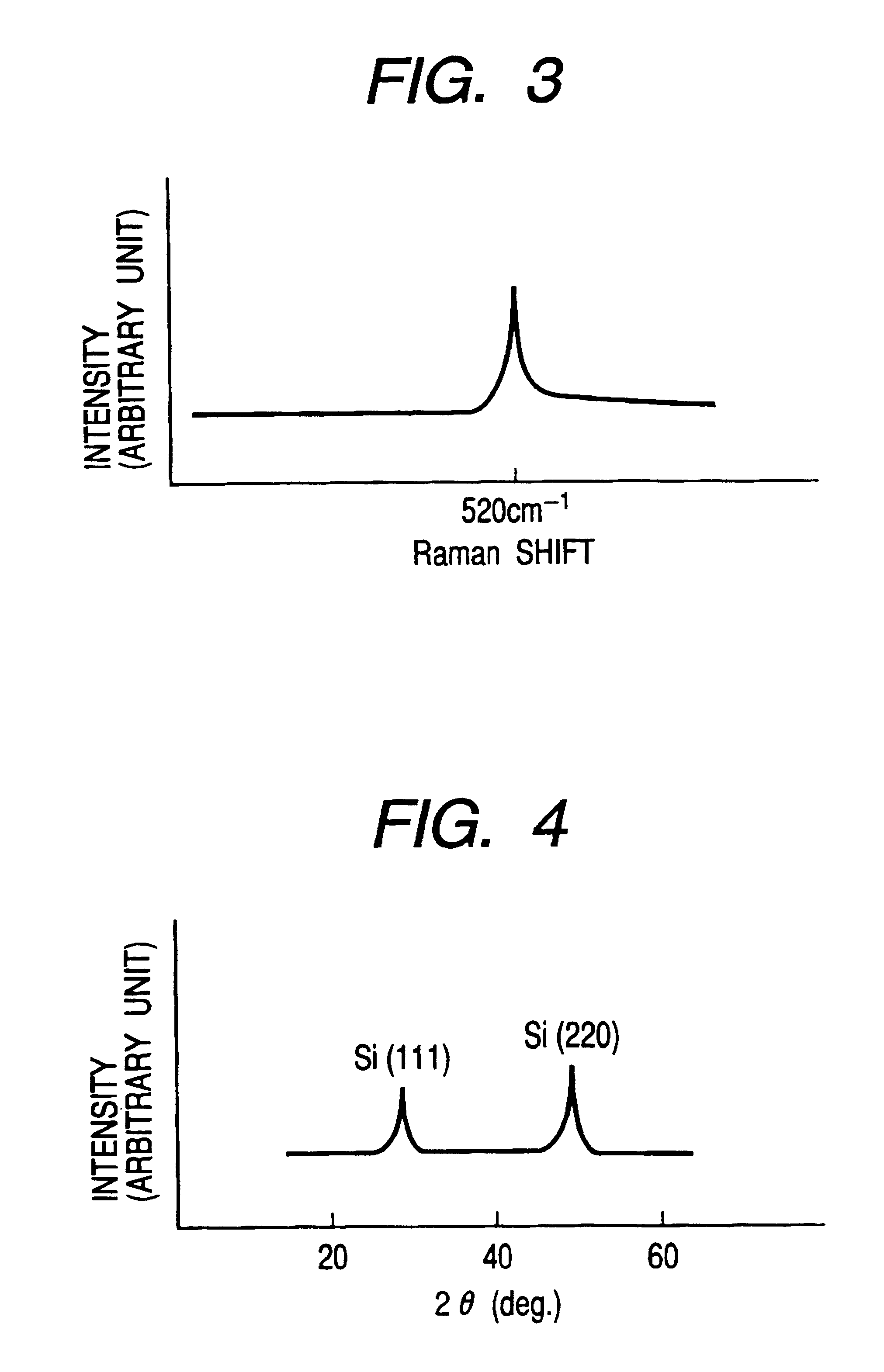
The deposited film was evaluated by the Raman scattering method and the X-ray diffractometry. As a result, the same results as in Comparative Example 1-1 were obtained, and so the deposited film was found to be crystallized. The crystal grain size found by using the Scherer's equation was about 250 .ANG. as to the peak (220).
example 1-2
A microcrystalline silicon film having a thickness of about 1 .mu.m was deposited on a 7059 glass substrate under the following conditions (frequency, f: 500 MHz; pressure, P: 0.03 Torr; residence time, .tau.: 4.2 ms; deposition rate: about 15 .ANG. / s). Forming conditions of the i-type layer (frequency, f: 500 MHz; pressure, P: 0.03 Torr; residence time, .tau.: 4.2 ms):
Gas flow rate: SiH.sub.4 =60 sccm, H.sub.2 =1,650 sccm
Deposition temperature: 350.degree. C.
VHF (105 MHz) power: 400 W
RF (13.56 MHz) power: 20 W
Deposition rate: about 15 .ANG. / S.
The deposited film was evaluated by the Raman scattering method and the X-ray diffractometry. As a result, the same results as in Comparative Example 1-1 were obtained, and so the deposited film was found to be crystallized. The crystal grain size found by using the Scherer's equation was about 150 .ANG. as to the peak (220).
example 1-3
Supply power was raised while retaining the residence time, .tau. of 32 ms in Example 1-1, thereby controlling the deposition rate to about 15 .ANG. / s that was the same rate as in Example 1-2. As a result, Raman scattering characteristics and X-ray diffraction characteristics similar to FIG. 3 and FIG. 4, respectively, were obtained even in Example 1-3. In any case, however, peak intensity was low compared with Example 1-1.
The crystal grain size estimated from the X-ray diffractometry in Example 1-3 was about 80 .ANG. that was considerably smaller than about 250 .ANG. in Example 1-1.
From the results of Comparative Examples 1-1 and 1-2 and Examples 1-1 to 1-3, it was confirmed that in a high deposition rate region of at least 5 .ANG. / s, the limitation of the residence time, .tau. to the range of .tau.<40 is advantageous to the provision of a microcrystalline silicon film having a greater crystal grain size. In particular, these results suggest that when the deposition rate is as very...
PUM
| Property | Measurement | Unit |
|---|---|---|
| power density | aaaaa | aaaaa |
| power density | aaaaa | aaaaa |
| pressure | aaaaa | aaaaa |
Abstract
Description
Claims
Application Information