
Highly compact EPROM and flash EEPROM devices

a high-compact, flash-type technology, applied in the direction of digital storage, instruments, transistors, etc., can solve the problems of difficult to prevent accidental tunneling, kynett's cell is more susceptible to low yield, and is far more susceptible to accidental "program disturb"

Inactive Publication Date: 2003-01-07
SANDISK TECH LLC
View PDF20 Cites 96 Cited by
  • Summary
  • Abstract
  • Description
  • Claims
  • Application Information

AI Technical Summary

Problems solved by technology

(c) Because of the presence of thin oxide layer between the floating gate and the drain diffusion, it is difficult to prevent accidental tunneling of electrons from the floating gate to the drain in what is known as the "program disturb" condition.
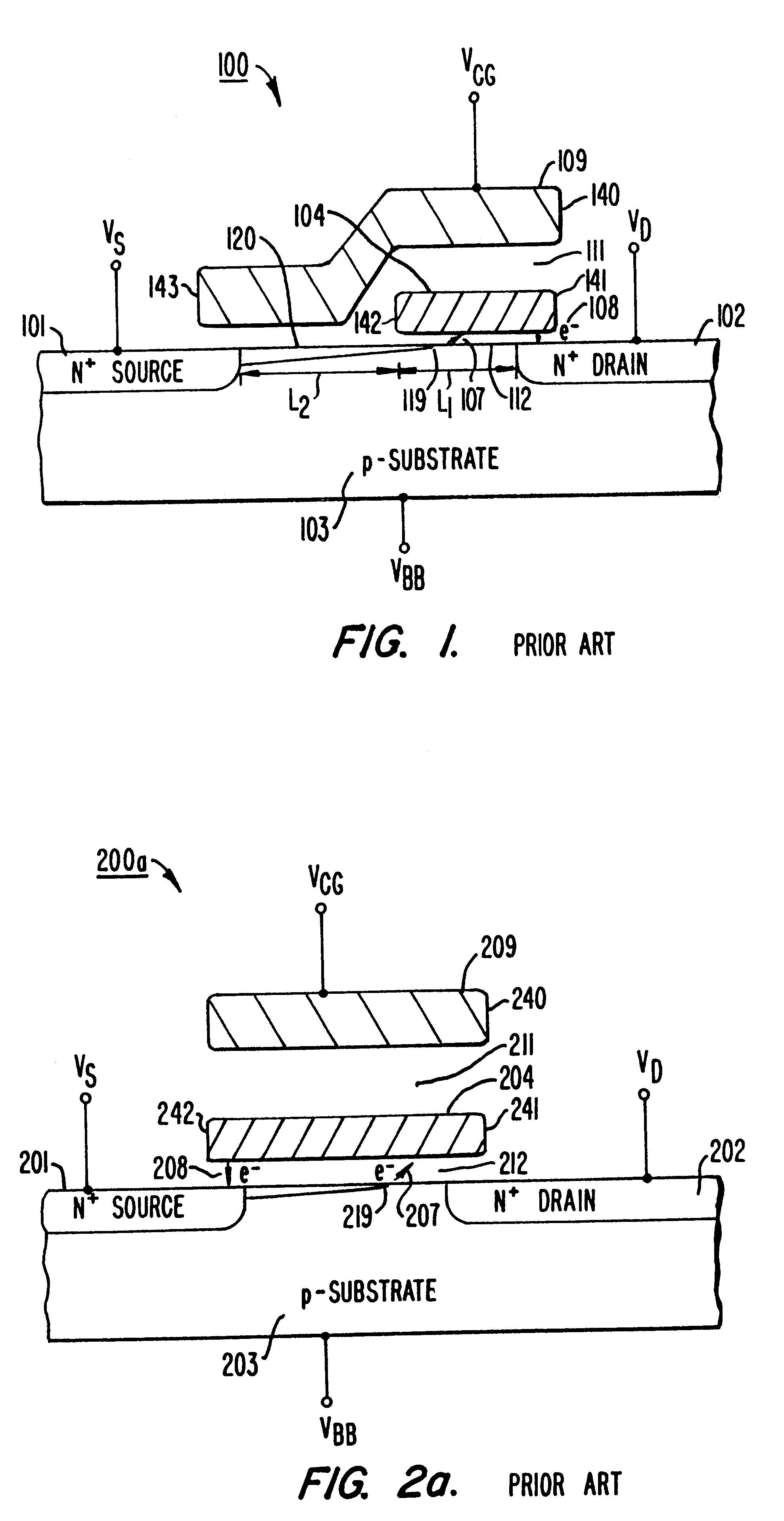
(a) Kynett is less susceptible to avalanche breakdown of source diffusion 201 during erase because the voltage is reduced from 19 volts to 12 volts.
(b) Kynett's cell is more susceptible to low yields due to pinholes in the thin dielectric layer 212 because its thickness is reduced from approximately 20 nanometers to approximately 10 nanometers.
(c) Because Kynett uses a lower voltage for erase but essentially the same drain voltage for programming Kynett is far more susceptible to accidental "program disturb" due to partial tunnel erase (during programming) occuring from floating gate 204 to drain 202.
(d) Kynett's cell is highly susceptible to an overerase condition because it does not have the series enhancement channel portion 120 of Samachisa's cell. To prevent overerase Kynett et al. deploy a special erase algorithm. This algorithm applies a short erase pulse to an array of cells, then measures the threshold voltage of all cells to ensure that no cell has been overerased into depletion. It then applies a second erase pulse and repeats the reading of all cells in the array. This cycle is stopped as soon as the last cell in the array has been erased to a reference enhancement voltage threshold level. The problem with this approach is that the first cell to have been adequately erased continues to receive erase pulses until the last cell has been adequately erased, and may therefore be susceptible to overerase into a depletion threshold state.
Gate dielectric 212 is relatively thick and does not permit tunnel erase from floating gate to source or drain.
This approach is extremely difficult to implement in a block erase of a large array because different transistors begin conduction at different times.
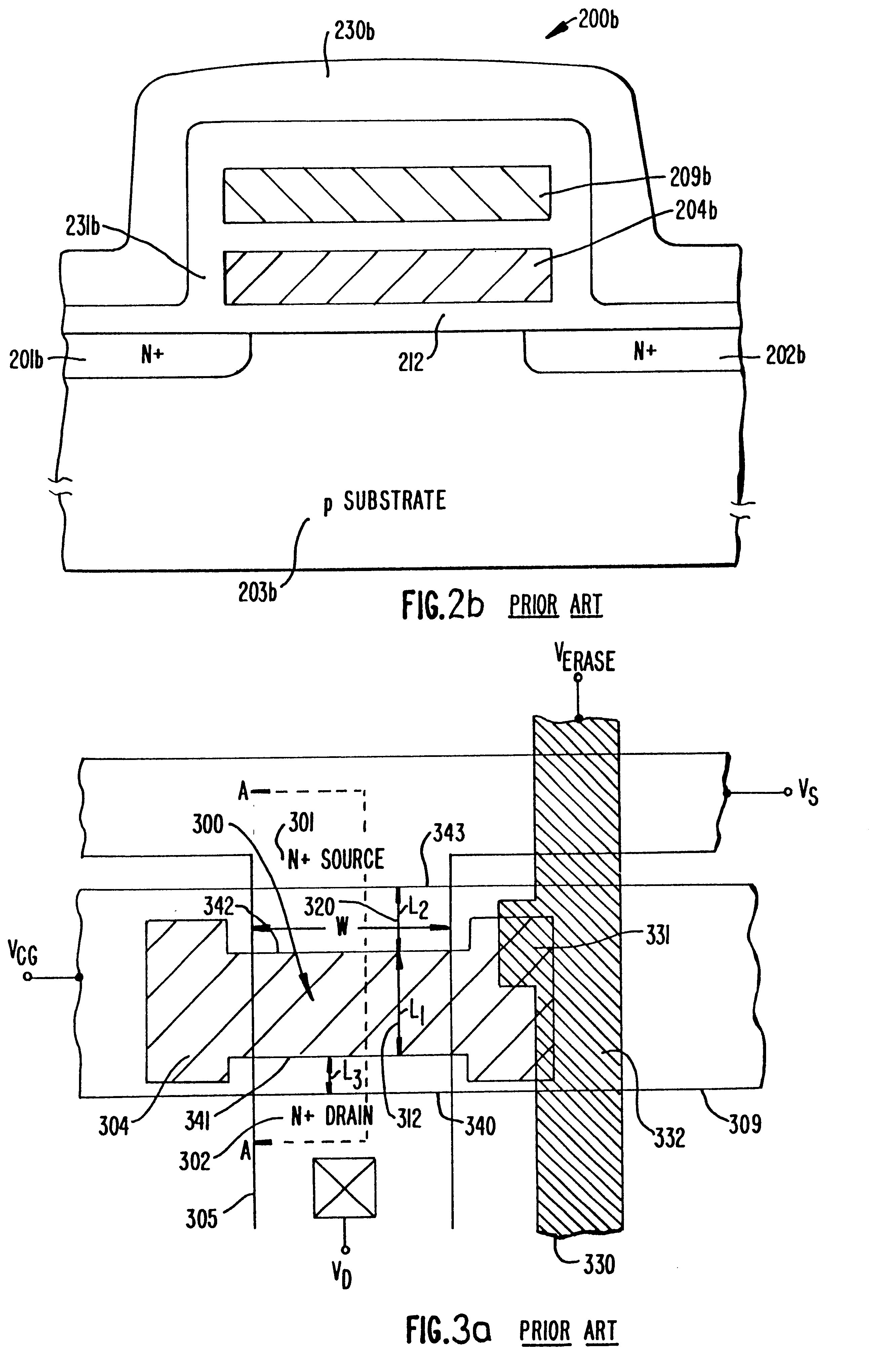
(a) Masuoka's cell does not erase by using either the source diffusion or the drain diffusion for tunnel erase. Therefore these diffusions never experience a voltage higher than during Eprom programming. The junction avalanche breakdown and junction leakage problems therefore do not exist.
(b) Masuoka's cell uses a relatively thick tunnel dielectric and therefore does not need to use thin tunnel dielectrics for erase. Therefore it is less susceptible to oxide pinholes introduced during the manufacturing cycle.
(c) Masuoka's cell does not have a "program disturb" problem because programming and tunnel erase involve two different mechanisms occuring at two different regions of the transistor.
(d) Masuoka's cell is not susceptible to the overerase condition because of the presence of the series enhancement transistor channel 320 (L2).
(e) Masuoka's cell requires a third layer of polysilicon, which complicates the process as well as aggravates the surface topology. Because the erase gate consumes surface area over the field oxide 305 it results in a larger cell.
(f) The overlap area 331 in Masuoka's cell is sensitive to mask misalignment between the two masks defining this overlap. Since the overlap area is nominally very small, even small misalignments can result in large variations in the area used for tunnel erase. This results in severe variations from wafer to wafer.
From the foregoing analysis it is clear that while the Masuoka prior art cell successfully addresses most of the problems encountered by Samachisa and Kynett, it itself has disadvantages not encountered by Samachisa or Kynett.
The disadvantages incurred by the addition of the series enhancement channel L2 are an increase in cell area, a decrease in transistor transconductance, an increase in control gate capacitance, and an increase in variability of device characteristics for programming and reading brought about by the fact that L1 or L2 or both are not precisely controlled in the manufacturing process of the prior art split channel devices.
It should be pointed out that even with the most advanced optical lithography systems available today in a production environment it is difficult to achieve an alignment accuracy of better than .+-.0.25 microns between any two mask layers.
Therefore, although the device achieves good control of L1 and L2 it is of rather low efficiency for both modes of operation.
Transistor 400e has proven difficult to manufacture because it is rather difficult to control the length Lp and the surface channel concentration p+ through a double diffusion step.
Furthermore, it is rather difficult to obtain value of Lp bigger than approximately 0.3 microns by diffusion because device scaling dictates the use of rather low temperature diffusion cycles.
Still further, the DSA Eprom device suffers from an excessively high transistor threshold voltage in the unprogrammed (conducting) state, as well as from high drain junction capacitance.
Both these effects can increase substantially the read access time.

Method used


Image

  • Highly compact EPROM and flash EEPROM devices
  • Highly compact EPROM and flash EEPROM devices
  • Highly compact EPROM and flash EEPROM devices

Examples


first embodiment

FIG. 5a presents a cross sectional view of a split channel Eprom transistor in accordance with this invention. Transistor 500a consists of a p type silicon substrate 563 (which can alternatively be a p type epitaxial layer grown on top of a p++ doped silicon substrate), N+ source diffusion 501a, N+ drain diffusion 502a, a channel region 560a which is more heavily p-doped than the surrounding substrate, a floating gate 504a overlying a portion L1 of the channel, 512a, and a control gate 509 overlying the remaining portion L2 of the channel, 520a as well as the floating gate. Floating gate 504a is dielectrically isolated from the surface of the silicon substrate by dielectric film 564a, which is thermally grown Silicon Dioxide. Control gate 509 is capacitively coupled to floating gate 504a through dielectric film 567a, which can either be thermally grown Silicon Dioxide or a combination of thin layers of Silicon Dioxide and Silicon Nitride. Control gate 509 is also insulated from the ...

second embodiment

FIG. 14c presents a cross sectional view of a non self aligned split channel Eprom transistor in accordance with this invention. FIGS. 14a and 14b illustrate the critical process steps in the manufacturing process of this device. Transistor 1400 consists of a p type silicon substrate 1463 (which can also be a p type epitaxial layer grown on a p++ substrate). Shallow N+ source diffusions 1401 and N+ drain diffusions 1402 are formed prior to formation of floating gate 1404, in contrast with the embodiment of section Ia above. The channel region between the source and drain diffusions is split into two portions: a portion L1 (1412) which is lying directly underneath the floating gate, and a portion L2 (1420) which is lying directly underneath the control gate 1409. The improvement over the Harari prior art split channel transistor 300d (FIG. 3d) consists of a heavily p+ doped narrow region 1460 adjacent to drain diffusion 1402. The width Lp (1413) and doping concentration of this regio...

third embodiment

Another embodiment of the self aligned split channel Flash EEprom of this invention can result in a cell which has smaller area than cells 600a and 700a of the embodiments described in Sections II and III respectively. In this third embodiment the area for tunnel erase between the floating gate and the erase gate is confined essentially to the surfaces of the vertical sidewalls along the two edges of each floating gate. To best understand how cell 800a of this embodiment differs from cell 700a a 2.times.2 array of cells 800a, 800b, 800c and 800d are shown in FIG. 8a in topological view and in FIG. 8b along the same cross section direction AA as is the case in FIG. 7b for cells 700a, 700c.

Cell 800a has a floating gate 804a formed in a first layer of heavily N+ doped polysilicon. This gate controls the transistor conduction in channel portion L1 (FIG. 8a) through gate oxide insulation film 864. Control gate 809 is formed in the second conductive layer, and is insulated from the floati...


PUM


Abstract

Structures, methods of manufacturing and methods of use of electrically programmable read only memories (EPROM) and flash electrically erasable and programmable read only memories (EEPROM) include split channel and other cell configurations. An arrangement of elements and cooperative processes of manufacture provide self-alignment of the elements. An intelligent programming technique allows each memory cell to store more than the usual one bit of information. An intelligent erase algorithm prolongs the useful life of the memory cells. Use of these various features provides a memory having a very high storage density and a long life, making it particularly useful as a solid state memory in place of magnetic disk storage devices in computer systems.

Description

This invention relates generally to semi-conductor electrically programmable read only memories (Eprom) and electrically erasable programmable read only memories (EEprom), and specifically to semiconductor structures of such memories, processes of making them, and techniques for using them.An electrically programmable read only memory (Eprom) utilizes a floating (unconnected) conductive gate, in a field effect transistor structure, positioned over but insulated from a channel region in a semi-conductor substrate, between source and drain regions. A control gate is then provided over the floating gate, but also insulated therefrom. The threshold voltage characteristic of the transistor is controlled by the amount of charge that is retained on the floating gate. That is, the minimum amount of voltage (threshold) that must be applied to the control gate before the transistor is turned "on" to permit conduction between its source and drain regions is controlled by the level of charge on...

Claims


Application Information

Patent Timeline
Patent Type & Authority Patents(United States)
IPC IPC(8): G11C16/06G11C16/04H01L21/28H01L21/70G11C11/56G11C16/34H01L29/66H01L21/02G11C29/00H01L27/115H01L21/8247H01L29/788G11C11/34H01L21/336H10B69/00
CPCG11C11/5621G11C11/5628G11C11/5635G11C11/5642G11C16/0425G11C16/349G11C16/3495G11C29/765G11C29/82H01L21/28273H01L27/115H01L27/11517H01L27/11519H01L27/11521H01L29/66825H01L29/7881H01L29/7885H01L2924/0002G11C29/00G11C2211/5613G11C2211/5631G11C2211/5634G11C2211/5644Y10S438/964H01L2924/00H01L29/40114H10B41/00H10B41/10H10B69/00H10B41/30
Inventor HARARI, ELIYAHOU
Owner SANDISK TECH LLC
Learn More