Method of producing diamond film for lithography

a lithography and diamond technology, applied in the direction of photomechanical treatment originals, instruments, nuclear engineering, etc., can solve the problems of inability to achieve high evenness and uniformity, inability to achieve good reproducibility, and difficulty in film growth,

Inactive Publication Date: 2003-01-21
SHIN ETSU CHEM IND CO LTD +1
View PDF9 Cites 11 Cited by
  • Summary
  • Abstract
  • Description
  • Claims
  • Application Information

AI Technical Summary

Benefits of technology

As described above, if a diamond film for lithography is formed by the method that a ground film is formed on a silicon substrate, a diamond film is formed on the ground film using a mixed gas of methane gas, hydrogen gas and oxygen gas as a raw material gas, and then the silicon substrate is removed by etching treatment, followed by removal of the ground film by etching treatment, a film can be produced without degrading smoothness, membrane stress or the like. Accordingly, a diamond film optimal as a mask membrane for lithography with X-ray or electron beam or the like can be produced.
According to the present invention, a diamond film having high crystallinity and desired membrane stress can be formed on the substrate, and a diamond film for lithography with X-ray or electron beam can be produced without degrading smoothness or membrane stress or the like after film formation.

Problems solved by technology

However, even though the diamond film is produced in accordance with the method for production, growth of the film is sometimes difficult, since a nucleus of diamond is hardly generated.
However, there are problems that surface processing cannot be conducted in high evenness and uniformity nor in good reproducibility.
However, in the method, sufficient density of nucleus generation cannot be obtained and sufficient thickness of the film cannot be obtained in some cases, and uniformity of the film is sometimes insufficient.
Therefore, all of the above-mentioned characteristics cannot be satisfied even by the method.
If the film is formed with low concentration of methane in the raw material gas, good crystallinity can be achieved, but tensile stress of the film is lowered, and thus the film has compressive stress and cannot be freestanding film.
As described above, it is quite difficult to produce a film having both of sufficient crystallinity and desirable membrane stress property that are basic properties of a diamond film.
The causes thereof include interference of a lot of film formation parameters, since plasma is used in film formation.

Method used


Image

  • Method of producing diamond film for lithography
  • Method of producing diamond film for lithography
  • Method of producing diamond film for lithography

Examples


example

The following examples and comparative examples are being submitted to further explain the present invention. Example 1

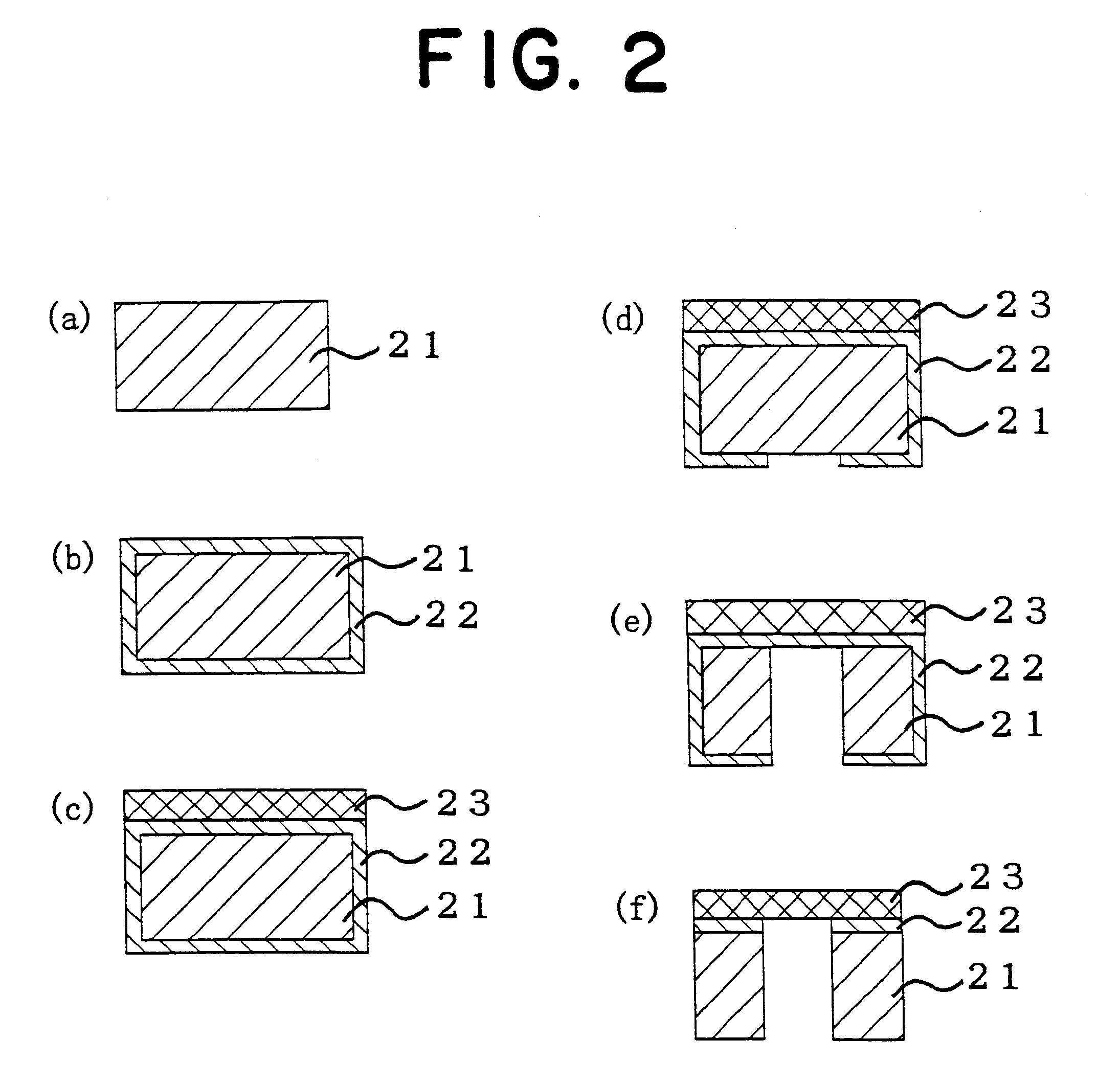
A double side polished silicon wafer (100) 21 having a diameter of 3 inches and a thickness of 2 mm was prepared as shown in FIG. 2(a). Then, on the surface thereof, a silicon nitride film 22 having a thickness of 0.5 .mu.m was formed according to a reduced pressure CVD method (FIG. 2(b)).

Before the diamond film 23 was formed on the silicon substrate 21 on which the silicon nitride film 22 was formed, the surface of the silicon nitride film 22 was treated with fluidized diamond particles in order to make generation of diamond nuclei easy.

After the above-mentioned treatment, the diamond film 23 was formed on the silicon substrate 21 on which the silicon nitride film 22 was formed (FIG. 2(c)).

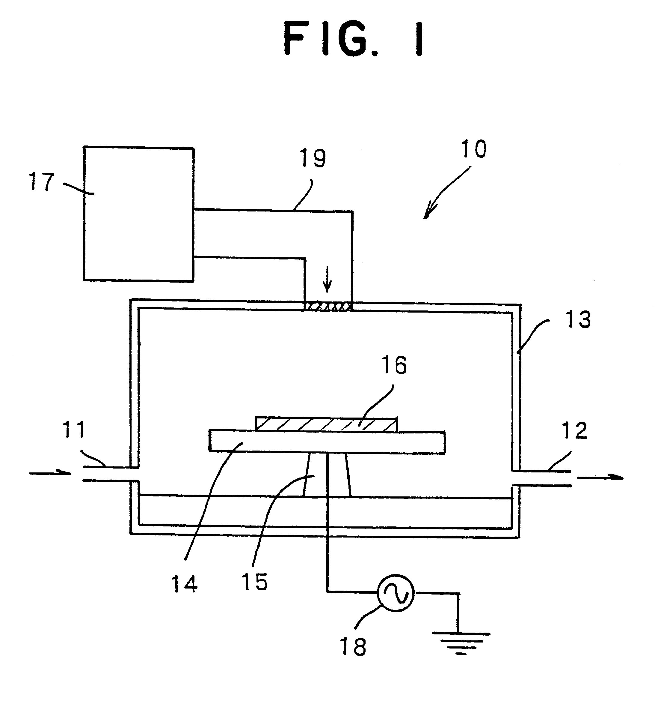
The diamond film 23 was formed using a microwave CVD apparatus shown in FIG. 1 as follows.

The silicon substrate 21 on which the silicon nitride film 22 (insulating film) of which...

example 3

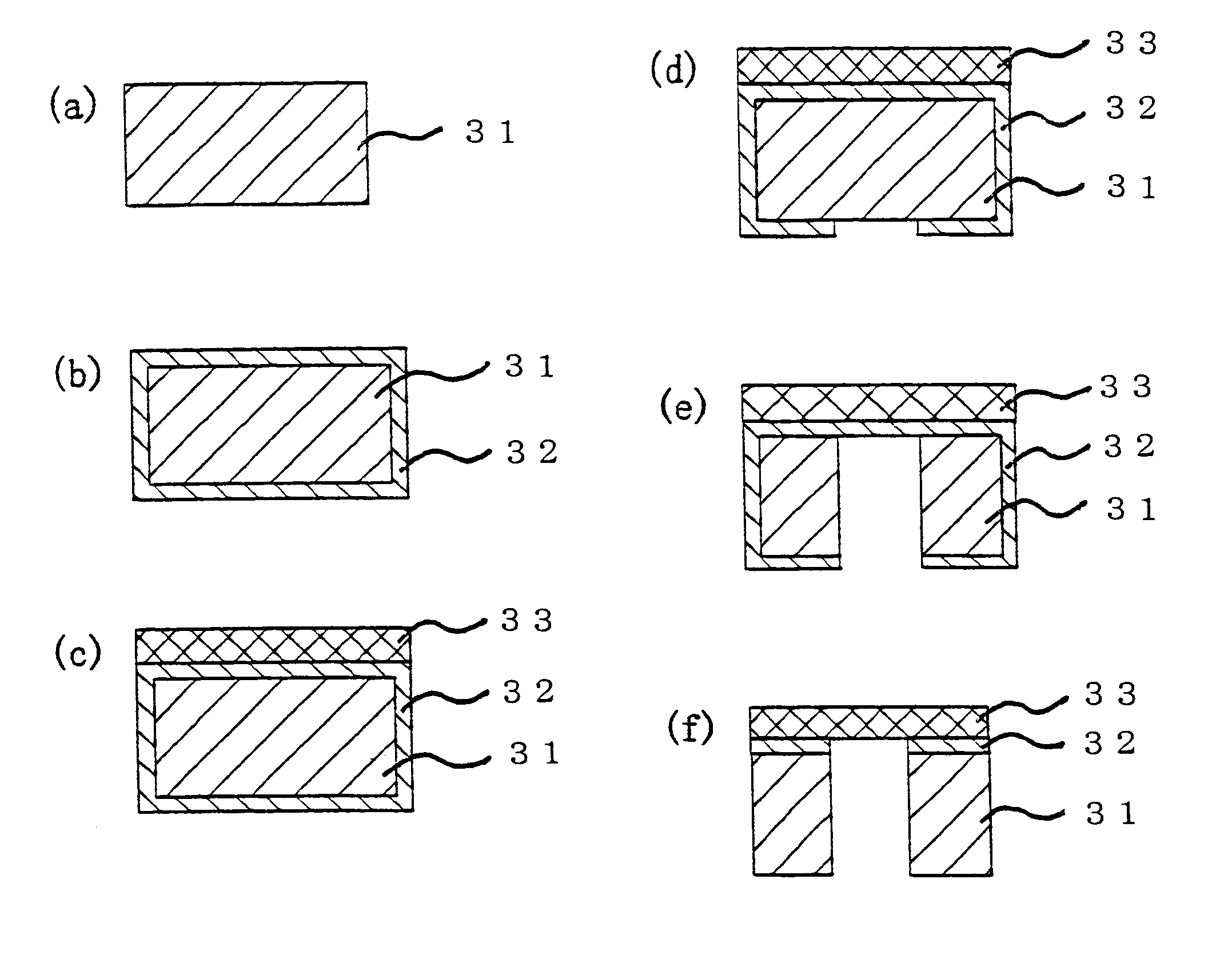
As shown in FIG. 3(a), double side polished silicon wafer (100) 31 having a diameter of 4 inches and a thickness of 600 .mu.m was prepared, and silicon nitride film 32 having a thickness of 0.5 .mu.m was formed thereon according to a reduced pressure CVD method (FIG. 3(b)). Then, the above-mentioned substrate was subjected to treatment with diamond particles through use of a diamond particle fluidizing apparatus shown in FIG. 4.

An acrylic tube having a inner diameter of 8 inches and a height of 1 m was used as a treatment chamber. 700 g of Synthetic diamond having an average particle size of 400 .mu.m was used as diamond particles. The wire netting made of stainless steal having a size of 40 .mu.m was used, through which nitrogen as a fluidizing gas was introduced from underneath. The nitrogen gas was introduced at a rate of 366 cm / sec that is 20 times as fast as Umf 18.3 cm / sec. The silicon substrate 31 on which silicon nitride film 32 was formed was fixed near the center of the tr...

example 4

The diamond particle fluidizing treatment was conducted under the same condition as Example 3 except that the ground substrate consisting of silicon nitride and having a diameter of 4 inches and a thickness of 600 .mu.m was used as a substrate. Then, the diamond film was formed on the substrate according to a microwave CVD method, to provide a polycrystalline diamond having a thickness of 1.2 .mu.m. The density of nucleus generation of the diamond film was 1.6.times.10.sup.8 / mm, 2.0.times.10.sup.8 / mm, 2.0.times.10.sup.8 / mm respectively at positions of 7 mm, 23 mm and 39 mm from the edge of the substrate. Accordingly, it was found that the film was extremely close and uniform.

Then, the part other than 30 mm square part at a center of the back surface of the substrate on which a diamond film was formed was masked with a resin film, and then the ground substrate was etched with an aqueous solution of hydrofluoric acid to a diamond film to provide membrane consisting of a diamond fil...


PUM

PropertyMeasurementUnit
temperatureaaaaaaaaaa
thicknessaaaaaaaaaa
pressureaaaaaaaaaa

Abstract

There is disclosed a method for producing a diamond film for lithography wherein a diamond film is formed on a silicon substrate on which an insulating film is formed or on an insulating substrate using a mixed gas of methane gas, hydrogen gas and oxygen gas as a raw material gas, and then the substrate is removed by etching treatment, and a method of producing a mask membrane for lithography wherein diamond particles fluidized with gas are brought into contact with a surface of a silicon substrate on which an insulating film is formed or an insulating substrate, a diamond film is grown on the substrate, and then the substrate is removed by etching treatment. There can be provided a method of producing a diamond film for lithography wherein a diamond film having high crystallinity and desired membrane stress can be formed on a substrate, and the film can be easily produced without degrading smoothness, membrane stress or the like after film formation.

Description

1. Field of the InventionThe present invention relates to a method of producing a diamond film (membrane) for lithography with X-ray, electron beam, or the like.2. Description of the Related ArtRecently, a semiconductor device has been highly accurate, and been highly integrated. In order to cope with the tendency, the pattern to be formed thereon is required to be finer, and lithography with X-ray or electron beam has been noted as a technique for realizing the requirement.In order to form the fine patterns, an exposure apparatus has been generally used in many cases. As material for a mask membrane attached to the exposure apparatus, diamond, boron nitride, silicon nitride, silicon carbide or the like are proposed. Among them, diamond is considered to be optimal as material of a mask membrane for lithography with X-ray or electron beam, since it is excellent in Young's modulus, etching resistance, high energy ray radiation resistance, or the like.As a method of producing a film, t...

Claims


Application Information

Patent Timeline
Patent Type & Authority Patents(United States)
IPC IPC(8): C23C16/00C23C16/26C23C16/01C23C16/02C23C16/27G03F1/14G03F1/16H01L21/20G03F1/20
CPCC23C16/01C23C16/0254G03F1/20C23C16/277C23C16/274H01L21/20
Inventor NOGUCHI, HITOSHIKUBOTA, YOSHIHIROOKADA, IKUO
Owner SHIN ETSU CHEM IND CO LTD
Why Eureka
Try Eureka