
Semiconductor device and a method of manufacturing the same

Inactive Publication Date: 2003-03-04
RENESAS ELECTRONICS CORP
View PDF5 Cites 36 Cited by
  • Summary
  • Abstract
  • Description
  • Claims
  • Application Information

AI Technical Summary

Benefits of technology

A specific object of this invention is to provide a technique capable of decreasing the on-resistance of a semiconductor device.
As the result, when the on-resistance is compared between the P type gate device and the N type gate device under an identical breakdown voltage, it is possible to effectively decrease the resistance in the P type gate device than in the N type gate device. That is, P type gate power MOSFET can improve the power-added efficiency.

Problems solved by technology

However, as described also in this literature, the unit wafer cost in the GaAs technique is more expensive compared with Si.
Usually, as the gate length is shorter, carrier velocity is saturated remarkably making it difficult to supply a great amount of current.

Method used


Image

  • Semiconductor device and a method of manufacturing the same
  • Semiconductor device and a method of manufacturing the same
  • Semiconductor device and a method of manufacturing the same

Examples


embodiment 1

of this invention is to be explained with reference to FIG. 1 through FIG. 5.

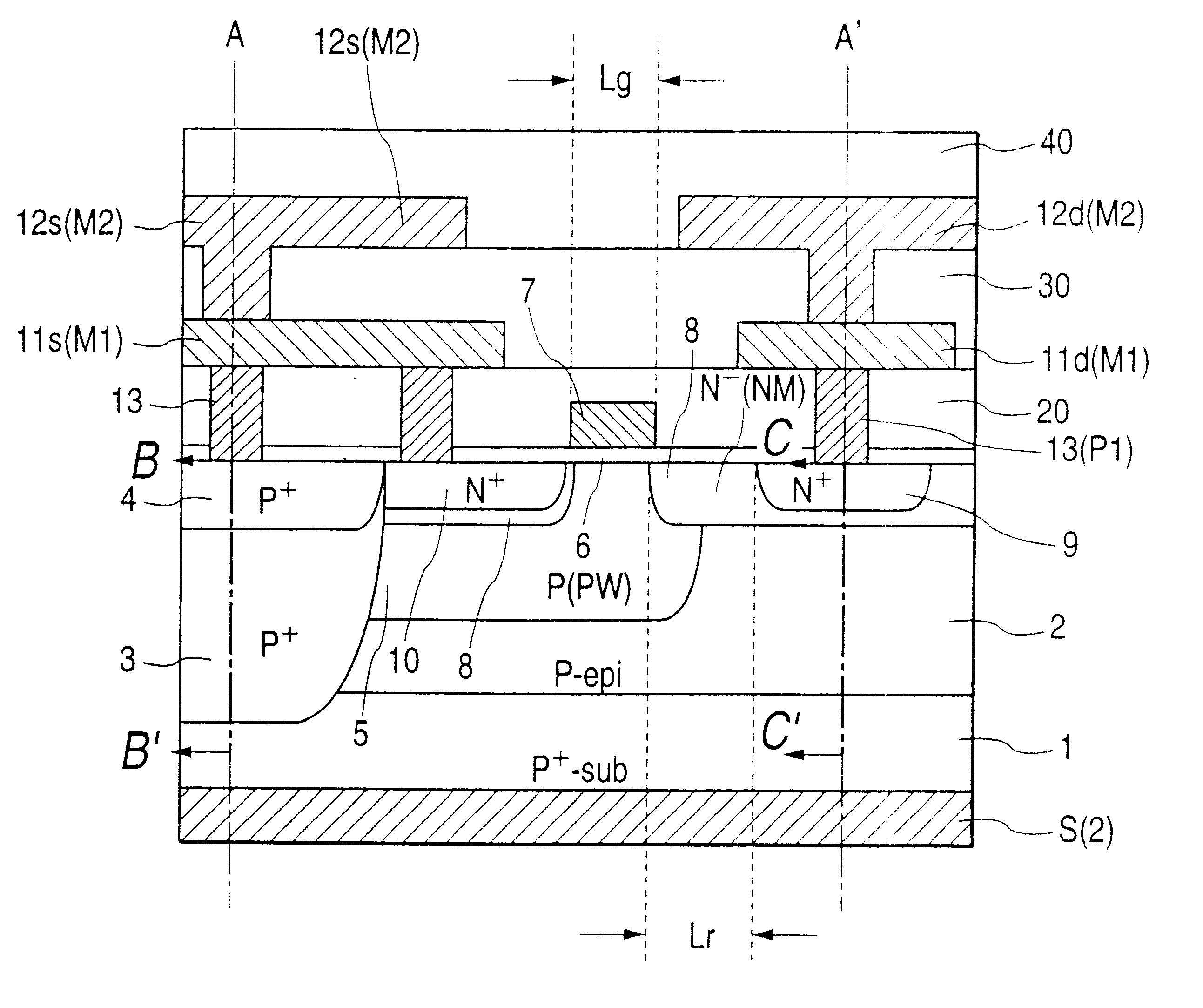
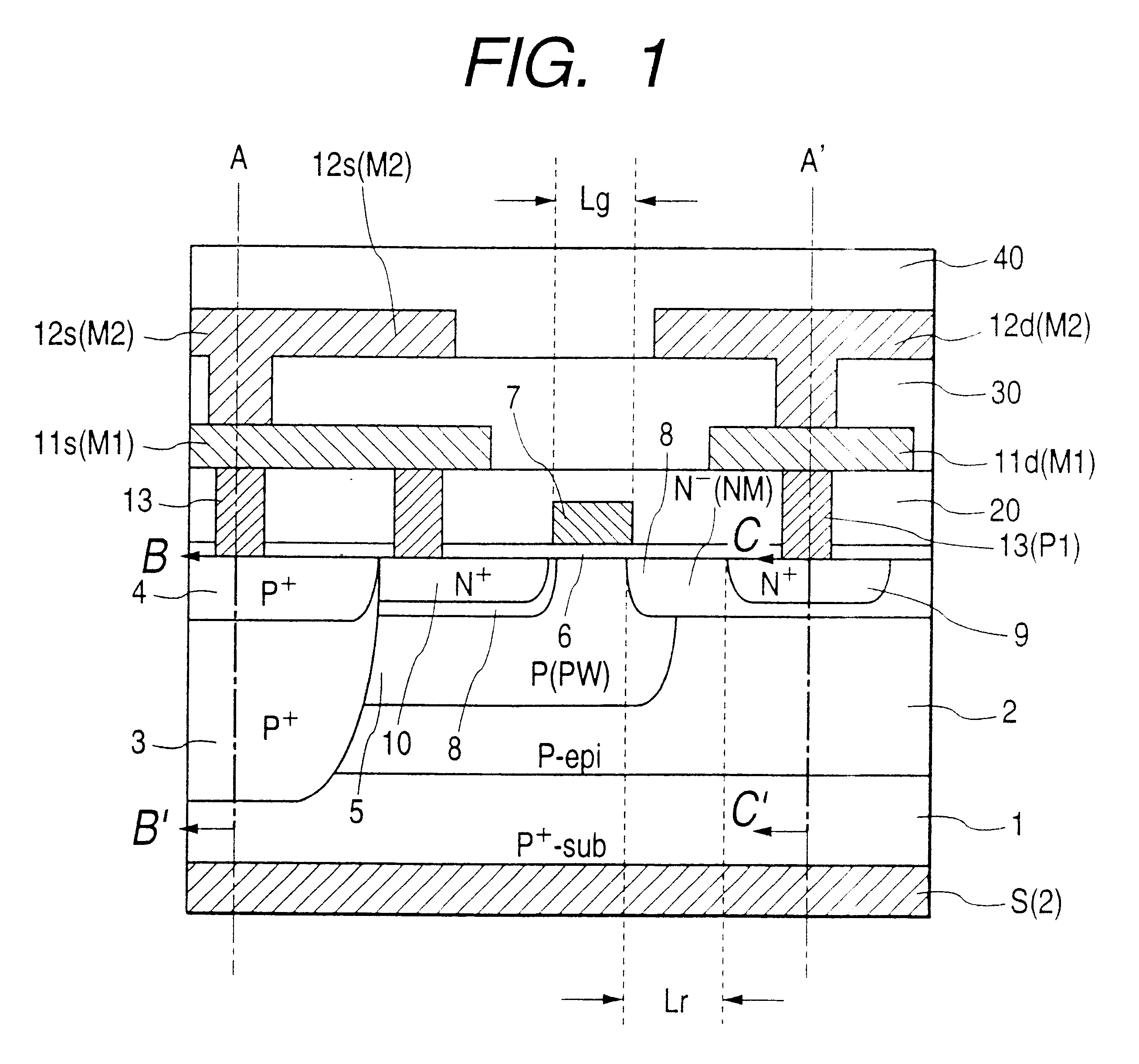
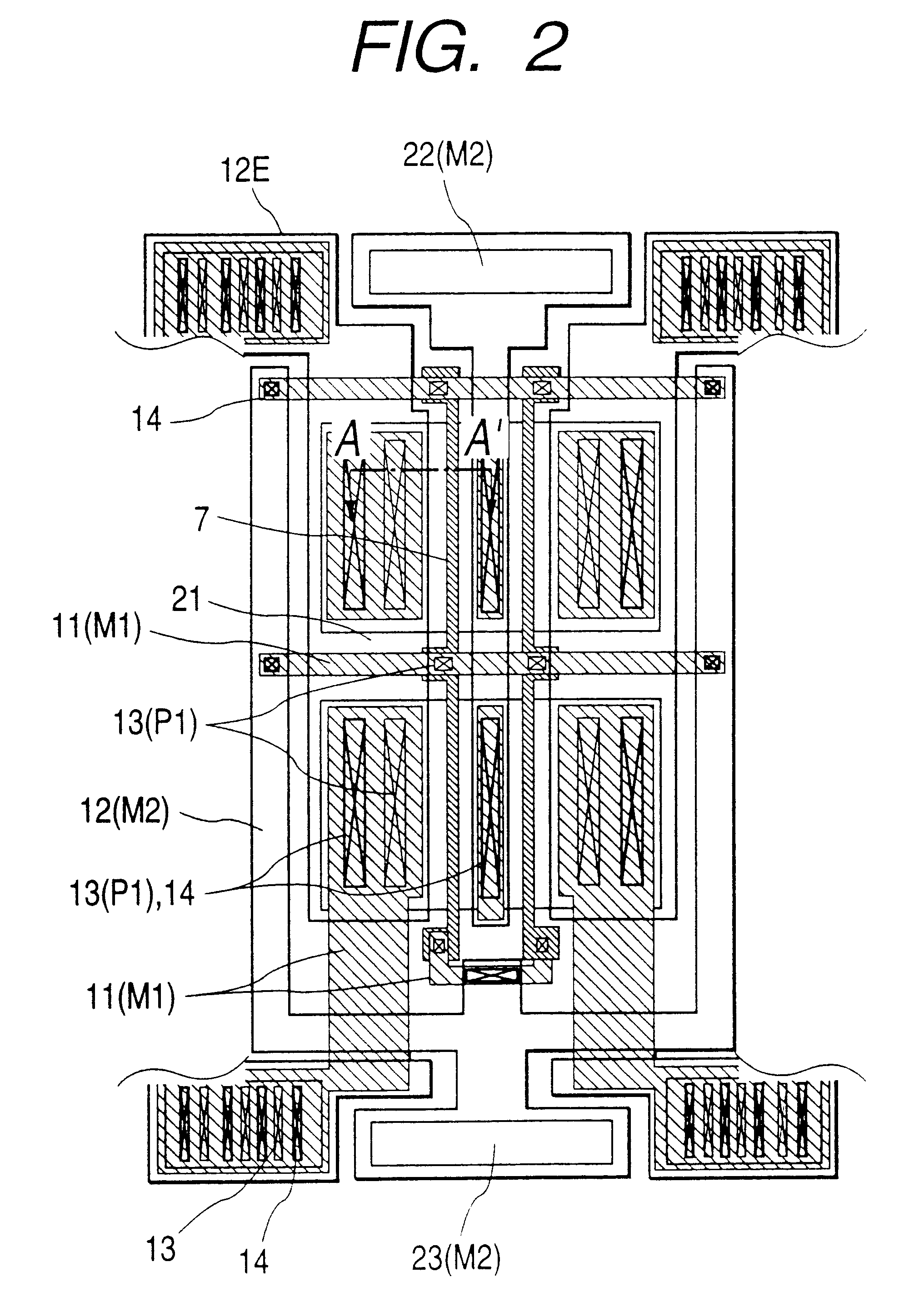
FIG. 1 is a cross sectional view of a semiconductor device (N gate N channel type Si power MOSFET) as Embodiment 1 according to this invention; FIG. 2 is a plan view of a semiconductor device as Embodiment 1 according to this invention; FIG. 3 is a plan view illustrating a layout of a semiconductor device (semiconductor chip) as Embodiment 1 according to this invention; FIG. 4 is an enlarged fragmentary plan view for a portion of a protection device 19 in the semiconductor device (semiconductor chip) shown in FIG. 3; and FIG. 5 is a cross sectional view taken along line D-D' for the protection device shown in FIG. 4.

A semiconductor device (basic cell of MOSFET) as Embodiment 1 according to this invention shown in FIG. 1 has the following constitution.

A P type high resistance Si epitaxy layer (first conduction type semiconductor layer) 2 is formed on the upper surface of a P type low resistance Si substrate ...

embodiment 2

In Embodiment 2, the oxide thickness of the gate electrode on both sides of the drain and the source is increased but the purpose can be attained by increasing the thickness only on the side of the drain. The embodiment for this constitution is to be explained later.

Succeeding to the step (9) for Embodiment 1 (refer to FIG. 12), the following steps are conducted.

(9-1) As shown in FIG. 54, an oxide film 21 is formed selectively by thermal oxidation. In this step, bird's beak is formed at the end of the gate electrode. That is, an oxide film (maximum thickness: 30 nm) of a thickness greater than the gate oxide film (10 nm thickness) is formed below the gate electrode end.

(9-2) Successively, as shown in FIG. 55, impurities are introduced through the silicon oxide film 21 for forming a drain offset region. That is, a low impurity semiconductor region (drain offset region) 8 is formed in self-alignment to the gate electrode 7 in the P well region 5 by ion implantation. Phosphorous as the...

embodiment 3

is a modification of Embodiment 2 in which the thickness for a portion of the gate oxide film of the gate electrode on the side of the drain is increased (refer to FIG. 60).

Succeeding to the step (9) of Embodiment 1 (refer to FIG. 12), the following steps are conducted. (9-1) As shown in FIG. 57, a silicon nitride film 200 is formed on a semiconductor substrate 1.

(9-2) Successively, as shown in FIG. 58, the silicon nitride film 200 is selectively removed so as to expose the end of the gate electrode on the side of the drain. Then, the gate bird's beak is formed only on the side of the drain by thermal oxidation using the silicon nitride film 200 as a mask.

(9-3) Successively, as shown in FIG. 59, impurities are introduced through a silicon oxide film 21 for forming a drain-offset region. That is, a low impurity semiconductor region (drain-offset region) 8 is formed in self alignment to a gate electrode 7 into a P type well region 5 by ion implantation.

Successively, the process from t...


PUM


Abstract

In a high frequency amplifying MOSFET having a drain offset region, the size is reduced and the on-resistance is decreased by providing conductor plugs 13 (P1) for leading out electrodes on a source region 10, a drain region 9 and leach-through layers 3 (4), to which a first layer wirings 11a, 11d (M1) are connected and, further, backing second layer wirings 12a to 12d are connected on the conductor plugs 13 (P1) to the first layer wirings 11s, 11d (M1).

Description

1. Field of the InventionThis invention concerns a semiconductor device used for mobile communication apparatus such as cellulars operation in a microwave band of 500 MHz to 2.5 GHz and, more in particular, it relates to a technique which is effective to high frequency powers amplifier of power-amplifying high frequency signals and outputting them.2. Description of Related ArtIn recent years, mobile communication apparatus typically represented by communication systems such as GSM (Global System for Mobile Communication), PCS (Personal Communication system), PDC (Personal Digital Cellular) system and CDMA (Code Division Multiple Access) system (so-called hand set telephone) have been popularized world wide.Generally, a mobile communication apparatus comprises an antenna for emitting and receiving electromagnetic waves, a high frequency power amplifier for amplifying high frequency signals under power modulation and supplying them to the antenna, a receiving section for processing hi...

Claims


Application Information

Patent Timeline
IPC IPC(8): H01L21/02H01L21/336H01L23/482H01L23/48H01L29/78H01L29/66H01L23/532H01L29/40H01L23/52H01L29/417H01L21/8234H01L27/04H01L27/088
CPCH01L21/823475H01L21/823871H01L23/4827H01L27/088H01L29/66659H01L29/7835H01L2924/0002H01L23/53219H01L23/53295H01L27/0255H01L29/0692H01L29/0696H01L29/0847H01L29/1045H01L29/105H01L29/1083H01L29/4175H01L29/41758H01L29/42368H01L29/4238H01L29/4916H01L29/861H01L2924/3011H01L2924/00H01L29/086H01L29/78
Inventor HOSHINO, YUTAKAIKEDA, SHUJIYOSHIDA, ISAOKAMOHARA, SHIROKAWAKAMI, MEGUMIMIYAKE, TOMOYUKIMORIKAWA, MASATOSHI
Owner RENESAS ELECTRONICS CORP
Learn More