Semiconductor manufacturing method

Inactive Publication Date: 2003-04-29
SHARP KK
View PDF11 Cites 13 Cited by
  • Summary
  • Abstract
  • Description
  • Claims
  • Application Information

AI Technical Summary

Benefits of technology

can be set to a large one. For example, when the thickness of the sacrifice film is set equal to the thickness of the crystalline silicon film, the volume ratio VR between gettering region and gettered region is necessarily beyond 1. Also, when the thickness of the sacrifice layer is set thicker than the thickness of the crystalline silicon film, the volume ratio VR between gettering region and gettered region can be set to an even larger one. Accordingly, the catalytic element in the gettered region can be reduced sufficiently. As a result of this, TFTs using this crystalline silicon film (gettered region) can be made excellent in electrical characteristics and reliability. Further, the area of the opening-correspondent portion of the crystalline silicon film can be reduced proportionally to the extent to which the getterability has improved over the prior art, so that the area of the crystalline silicon film (gettered region) left on the substrate can be enlarged. Accordingly, TFTs arrangement on the substrate is not limited in their layout.
With this semiconductor manufacturing method of one embodiment, the material of the sacrifice layer is any one of amorphous silicon, polysilicon and single crystal silicon, the sacrifice layer being formed principally from the silicon element as the crystalline silicon film is. By virtue of this homogeneity of material, the catalytic element can be gettered from the crystalline silicon film to the sacrifice film with high efficiency.
With this semiconductor manufacturing method of one embodiment, since the temperature of the second heat treatment is set to within a range of 500.degree. C. to 700.degree. C., the second heat treatment is performed at a relatively low temperature. Accordingly, deformation of the substrate and the like can be prevented. Further, the getter element is desirably one having a small diffusion coefficient, as compared with the catalytic element, at the temperature of the second heat treatment. This is because such a getter element does not diffuse into the mask layer but remains in the sacrifice layer during the second heat treatment, thus allowing the catalytic element to be gettered with high efficiency. In this semiconductor manufacturing method of one embodiment, since the temperature of the second heat treatment is set to within a range of 500.degree. C.-700.degree. C., it is easy to select such a getter element.
With this semiconductor manufacturing method of one embodiment, one kind of element or a plurality of kinds of elements selected from among nitrogen, phosphorus, arsenic, antimony and bismuth is used as the getter element. These elements, having a property of bonding with metallic elements, allow the metallic element as a catalyst to be gettered with high efficiency. As a result of this, the catalytic-element concentration in the gettered region can be reduced sufficiently.

Problems solved by technology

Although amorphous silicon is generally used as the material of TFTs, yet its electrical characteristics are much inferior to lower than those of single-crystalline semiconductors used in so-called silicon LSIs or the like.
However, polysilicon has limitations in electrical characteristics, not meeting the demand.
However, it cannot be neglected that the catalytic element remaining in the crystalline silicon film may have adverse effects on the electrical characteristics and reliability of the TFTs such as shifts of their threshold voltage and deterioration in hot carrier resistance.
Among these factors, with regard to (1), the larger the area of the gettering region 3 relative to the area of the gettered region 4 becomes, the more the getterability improves while, unfortunately, the region where TFTs can be formed is limited proportionally.
Therefore, the conventional method has a problem that the area of the gettered region 4, i.e. the area of the crystalline silicon film 2 left on the substrate 1, becomes smaller, so that the layout in the arrangement of the TFTs is limited.

Method used


Image

  • Semiconductor manufacturing method
  • Semiconductor manufacturing method
  • Semiconductor manufacturing method

Examples


Embodiment Construction

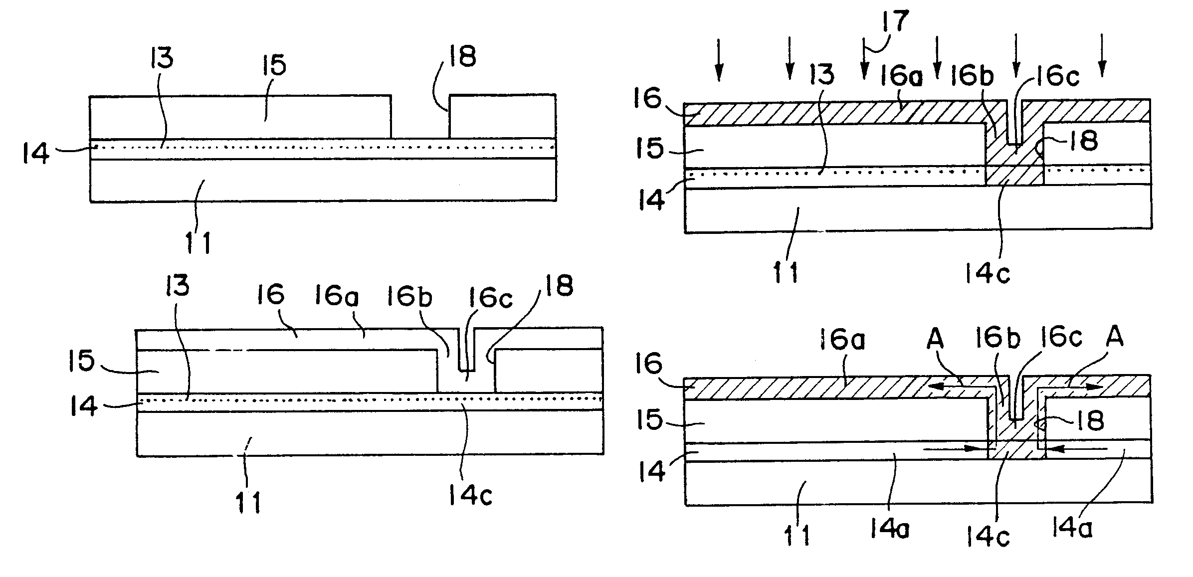
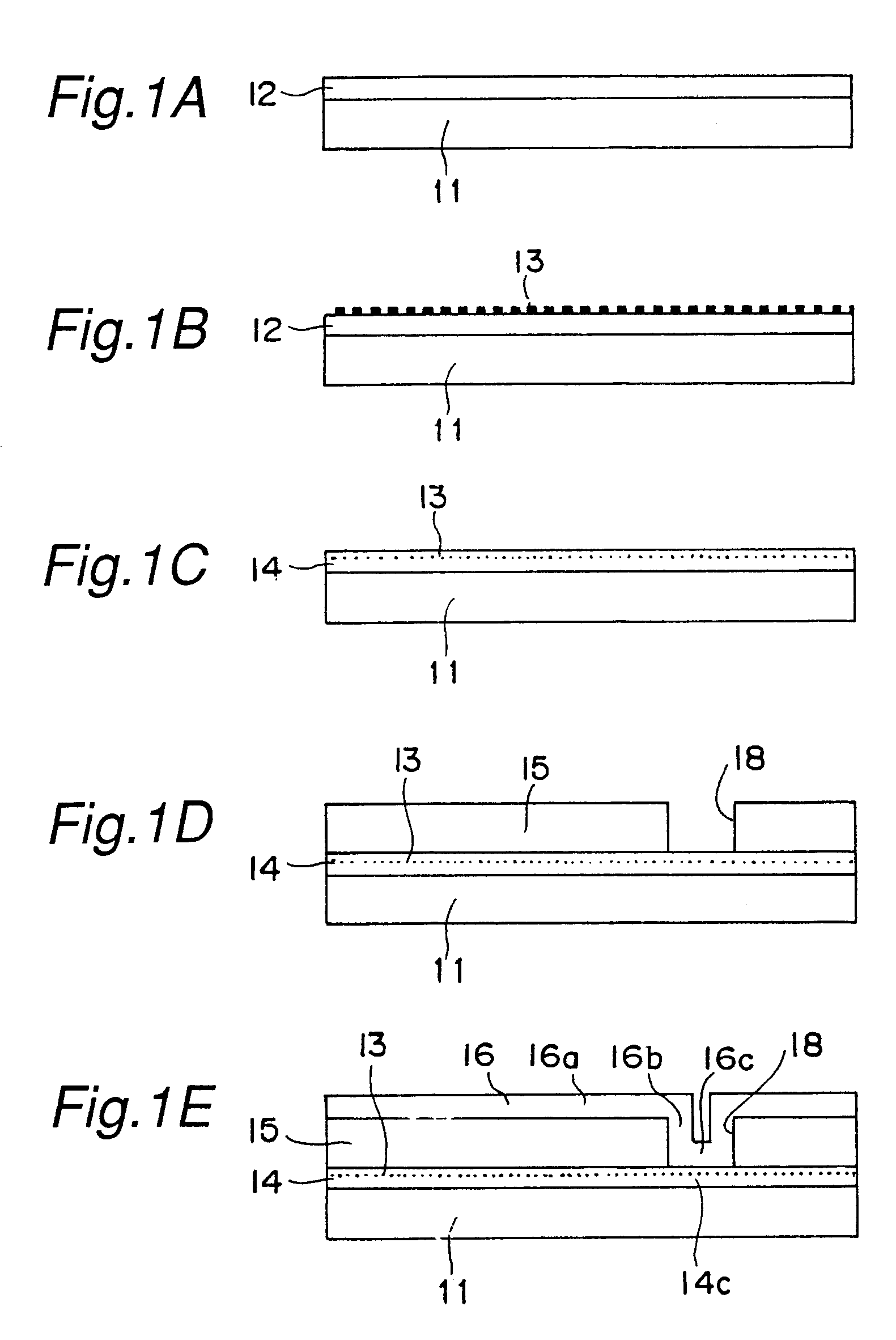
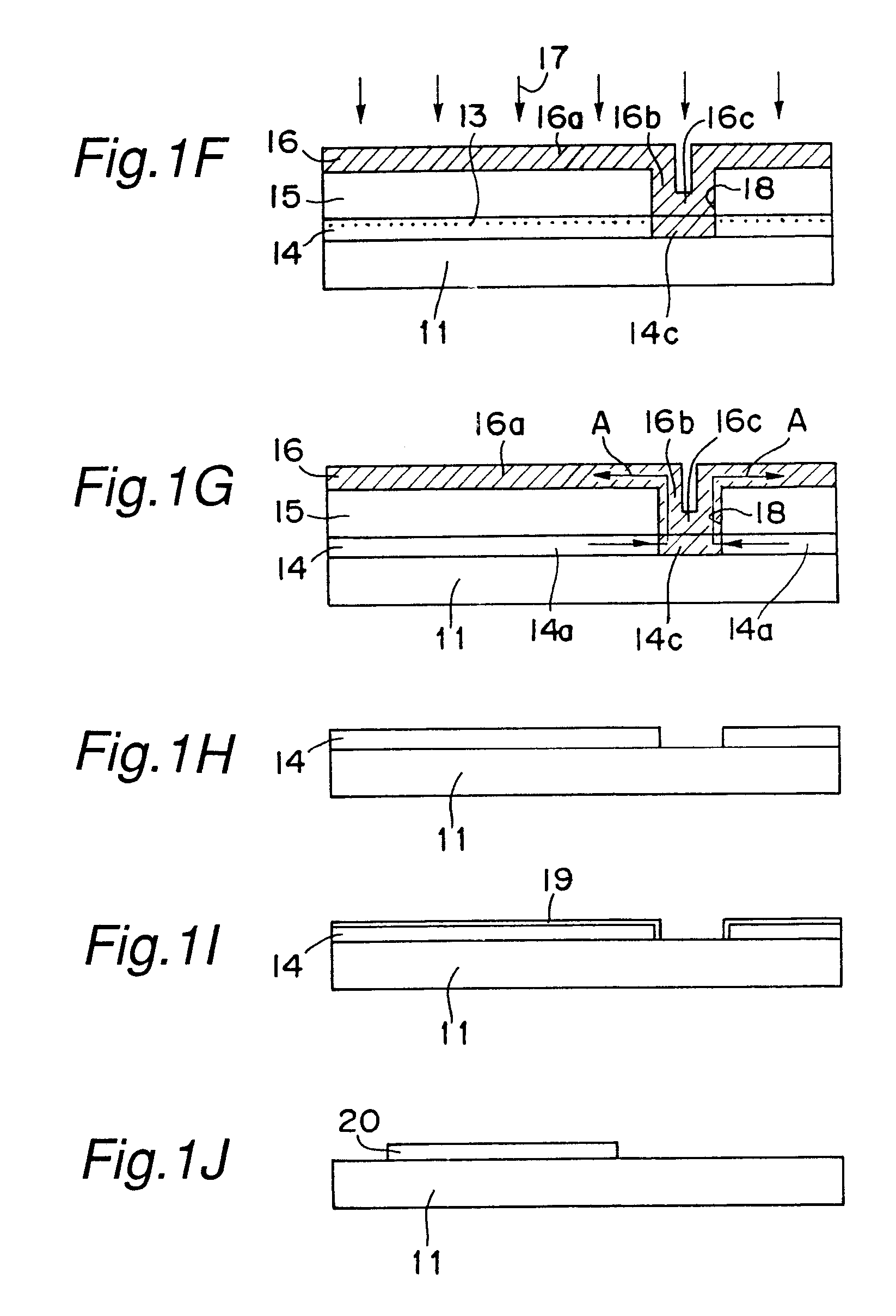
Hereinbelow, a semiconductor manufacturing method of the present invention is described in detail by way of an embodiment thereof illustrated in the accompanying drawings.

FIGS. 1A, 1B, 1C . . . 1M are sequentially show the steps of a TFT manufacturing method to which the present invention is applied. i) As shown in FIG. 1A, an amorphous silicon (.alpha.-Si) film 12 is deposited to a thickness of 70 nm on a quartz substrate 11 by LPCVD (low pressure chemical vapor deposition) process. Conditions for the growth are set to a temperature of 450.degree. C. and a pressure of 50 pa with the use of disilane gas (Si.sub.2 H.sub.6) as the material gas. ii) Next, as shown in FIG. 1B, an aqueous solution prepared by dissolving a metallic element, for example, Ni to 10 ppm into pure water is applied over the entire surface of the .alpha.-Si film 12 by spinning process. This Ni element acts as a catalyst for accelerating the crystallization of the .alpha.-Si film 12 in a heat treatment process, w...


PUM


Abstract

There is provided a semiconductor manufacturing method capable of sufficiently reducing catalytic element in a crystalline silicon film and also increasing the area of the crystalline silicon film to be left on the substrate. A catalytic element for accelerating the crystallization is introduced into an amorphous silicon film on a substrate, and a first heat treatment is performed to crystallize the amorphous silicon film into a crystalline silicon film. A mask layer is provided on the surface of the crystalline silicon film, the mask layer having an opening passing thicknesswise through the mask layer. Further thereon, a sacrifice film is formed so as to continuously cover the surface of the mask layer and an opening-correspondent portion of the crystalline silicon film. A getter element for gettering the catalytic element is introduced into the sacrifice film and the opening-correspondent portion of the crystalline silicon film. A second heat treatment is performed, by which the catalytic element is gettered from the crystalline silicon film to the sacrifice film through the opening.

Description

BACKGROUND OF THE INVENTIONThe present invention relates to a semiconductor manufacturing method and, more specifically, to a method for manufacturing a silicon semiconductor thin film having crystallinity. Silicon semiconductor thin films fabricated according to the semiconductor manufacturing method of the invention are suitably used as the material of TFTs (Thin Film Transistors) in active-matrix type LCDs (Liquid Crystal Displays) and various kinds of semiconductor devices.Although amorphous silicon is generally used as the material of TFTs, yet its electrical characteristics are much inferior to lower than those of single-crystalline semiconductors used in so-called silicon LSIs or the like. Therefore, in LCDs, TFTs are used exclusively as switching devices only, and not used for peripheral circuits to which high performance is demanded. Also, studies have been made on using polysilicon in place of amorphous silicon to improve the characteristics of TFTs. However, polysilicon h...

Claims


Application Information

Patent Timeline
IPC IPC(8): H01L21/20H01L29/786H01L21/336H01L29/66H01L21/02H01L21/322H01L21/205
CPCH01L21/2022H01L29/78675H01L29/66757H01L21/3226H01L21/0262H01L21/02532H01L21/02672H01L21/20
Inventor FUKUSHIMA, YASUMORI
Owner SHARP KK
Why Eureka
Try Eureka