

Large area organic electronic devices having conducting polymer buffer layers and methods of making same
a technology of organic electronic devices and buffer layers, which is applied in the direction of discharge tubes/lamp details, discharge tubes luminescnet screens, other domestic articles, etc., can solve the problems of becoming more and more difficult to control the number of defects on the substrate or electrode layer, and achieve the effects of improving the performance of oleds, reducing or eliminating performance failures, and increasing performance reliability
- Summary
- Abstract
- Description
- Claims
- Application Information
AI Technical Summary
Benefits of technology
Problems solved by technology
Method used
Image

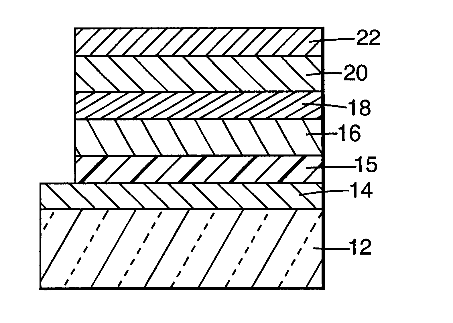
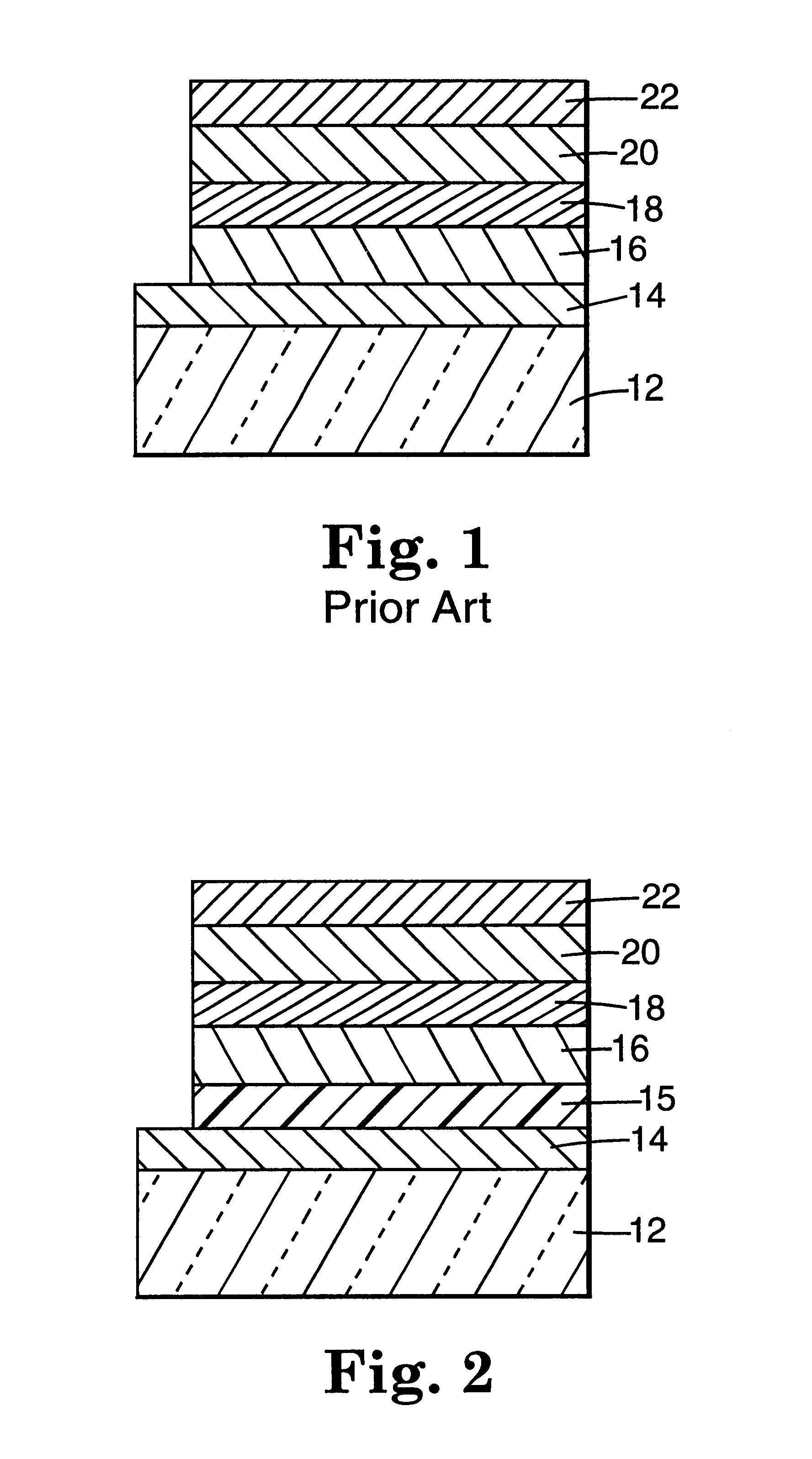
Examples
example 1
Externally-Doped Polyaniline on Flexible Substrate
ITO-coated poly(ethylene terephthalate) (PET) was prepared by treating about 7.6 m of 0.125 mm thick PET film, 15.2 cm wide, in a vacuum roll coater using DC planar magnetron sputtering at a pressure of 8.times.10.sup.-3 torr using a sputter gas of 95% argon and 5% oxygen. The ITO sputter target was a 99.99% pure ceramic comprising 90% In.sub.2 O.sub.3 and 10% SnO.sub.2, having a density of 90%. Sputtering took place at 280 watts and 350 volts, with a current of 0.80 amperes. The film was processed through the coater at a rate of 16 cm / min. The coated film exhibited a quarterwave reflectance maximum at 550 nm. Sheet resistance of the coated film ranged from 71 to 83 ohm / square.
The substrate was rinsed with deionized water, dried under a nitrogen stream, then placed in a micro-gravure coater (CAG-150-UV, Yasui Seiki USA Co., Bloomington, Ind.) equipped with a Tri-Helical roller (a Quad roller may alternatively be used) and a three-sta...
example 2
Coating of Self-Doped Polyaniline on Flexible Substrate
A flexible ITO-coated PET substrate (Southwall Technologies, Palo Alto, Calif.) measuring approximately 5 cm.times.15 cm was wiped clean with ethyl alcohol on a soft cloth, then soaked for 30 seconds in a metal ion-free developer solution (Shipley 319, Shipley Div. of Rohm and Haas, Marlboro, Mass.), then rinsed with deionized water. The substrate was clamped onto a glass plate in a flexographic ink proofing unit (The Precision Proofer, manufactured by Precision Proofing Co., West Monroe, La. and described in U.S. Pat. No. 4,984,532) that was equipped with a two-roll microgravure offset coating head (Precision Hand Proofer, Pamarco, Inc., Roselle, N.J.). A bead of unfiltered water-soluble 75% sulfonated self-doped polyaniline (Aldrich) was placed on the ITO-coated substrate in front of the microgravure roller and a coating of the polyaniline solution was applied to the substrate by moving the roller over the substrate at a const...
PUM
 Abstract
Description
Claims
Application Information