

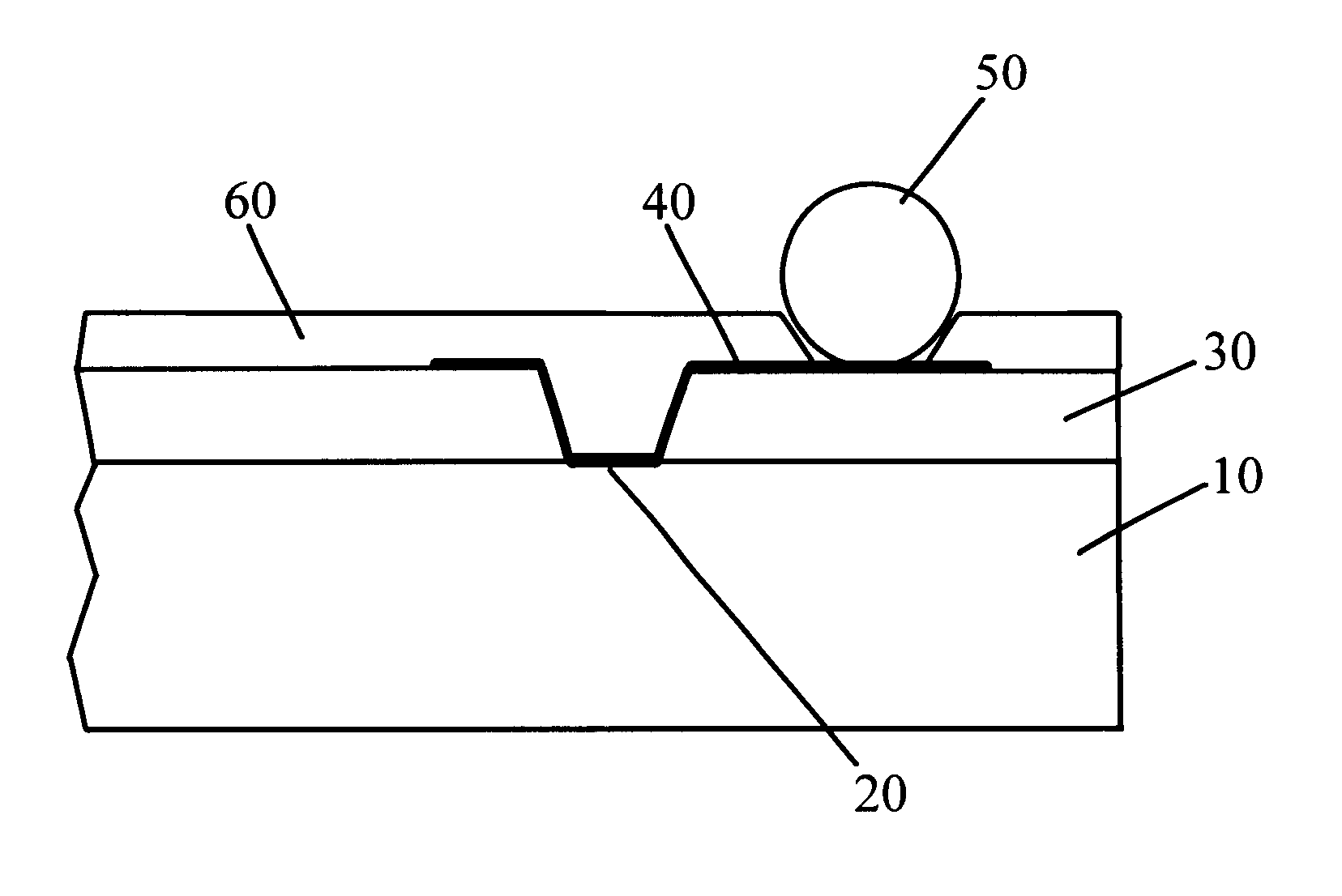
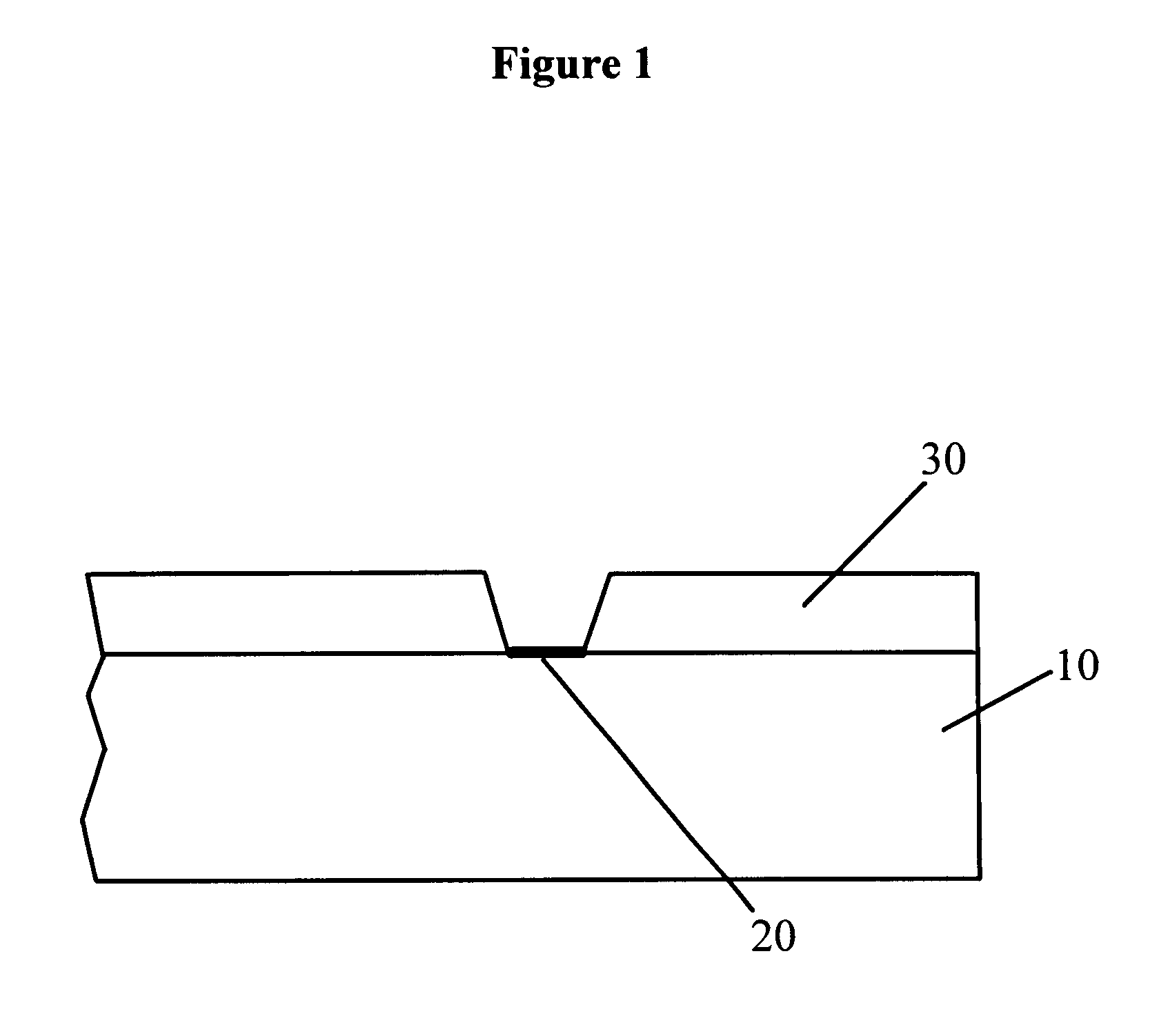
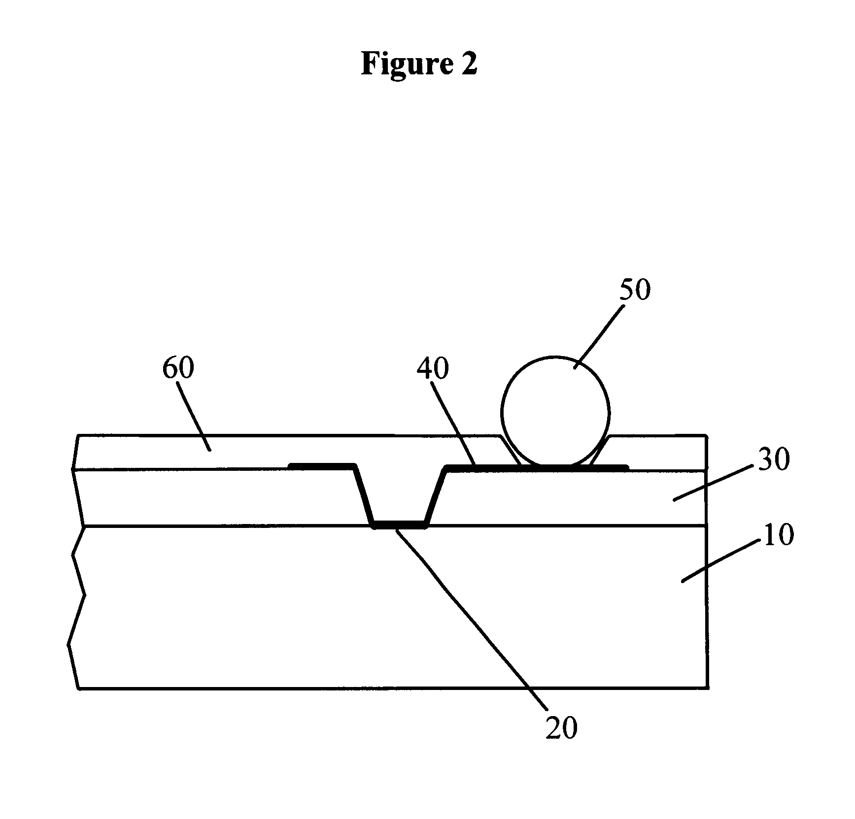
Semiconductor package and method of preparing same
a technology of semiconductors and components, applied in the field of semiconductor packages, can solve the problems of limited reliability of ic packages, and achieve the effects of good environmental resistance, good thermal stability, and high throughpu
- Summary
- Abstract
- Description
- Claims
- Application Information
AI Technical Summary
Benefits of technology
Problems solved by technology
Method used
Image

Examples
examples
The following examples are presented to further illustrate the method of photopatteming the silicone composition of this invention, but are not to be considered as limiting the invention, which is delineated in the appended claims. Unless otherwise noted, all parts and percentages reported in the examples are by weight. The following methods and materials were employed in the examples:
Irradiation of a silicone film was carried out using a OAI 7-inch medium pressure mercury projection lamp equipped with a 4-inch diameter interference filter centered at 365.+-.2 nm (I-line) and having a half-height peak width of 10.+-.2 nm (Optics Automation Instrumentation, Milpitas, Calif.). Radiation dose (mJ / cm.sup.2) was measured using an International Light radiometer calibrated against I-line radiation.
Thickness of a cured silicone film on a silicon wafer was determined using a Tencor P-11 surface profilometer (KLA Tencor, Milpitas, Calif.). Film thickness was measured at a step between the coa...
examples 1-3
Resin (46.84 parts), 42.16 parts of Crosslinking Agent, and 10.12 parts of mesitylene were combined in an amber bottle. Catalyst D (0.89 part) was added to the blend and mixing was continued for 0.5 h at room temperature. The mixture was then pressure-filtered (138 to 276 kPa nitrogen) through a stainless steel canister containing 10-.mu.m and 5-.mu.m nylon membranes in series. The silicone composition (filtrate) was stored prior to use at -15.degree. C. in a closed polyethylene bottle wrapped in aluminum foil.
In each of Examples 1-3, the silicone composition (about 2.5 g), which was at room temperature, was applied to a 100-mm silicon wafer and spun out into a thin film (500 rpm for 10 s followed by 3000 rpm for 30 s). The coated wafer was heated on a hot plate at 110.degree. C. for 2 minutes to remove most of the solvent. The film was then exposed to I-line radiation (365 nm) through a photomask containing 250-.mu.m circular apertures and in near contact with the film. The wafer w...
examples 4-33
In each of Examples 4-34, a silicone composition was prepared by combining the a silicone base with the Catalyst specified in Table 2 according to the following procedure: Silicone Base (99.15 parts) and 0.85 part of Catalyst were combined in an amber bottle and mixed for 0.5 h at room temperature. The mixture was then pressure-filtered (138 to 276 kPa nitrogen) through a stainless steel canister containing 10-.mu.m and 5-.mu.m nylon membranes in series. The silicone composition (filtrate) was stored prior to use at -15.degree. C. in a closed polyethylene bottle wrapped in aluminum foil.
A sample of the silicone composition (about 2.5 g), which was at temperature, was applied to a 100-mm silicon wafer and spun out into a thin film (500 rpm for 10 s followed by 3000 rpm for 30 s). The coated wafer was heated on a hot plate at 110.degree. C. for 2 minutes to remove most of the solvent. The film was then exposed to I-line radiation (365 nm) through a photomask containing 40-.mu.m circul...
PUM
| Property | Measurement | Unit |
|---|---|---|
| wavelength | aaaaa | aaaaa |
| thickness | aaaaa | aaaaa |
| mole ratio | aaaaa | aaaaa |
Abstract
Description
Claims
Application Information