Laser irradiation stage, laser irradiation optical system, laser irradiation apparatus, laser irradiation method, and method of manufacturing a semiconductor device

a laser irradiation and semiconductor technology, applied in semiconductor lasers, manufacturing tools, instruments, etc., can solve the problems of difficult semiconductor elements to be formed, uneven light intensity, and poor influence on throughput and footprin

Inactive Publication Date: 2004-03-16
SEMICON ENERGY LAB CO LTD
View PDF10 Cites 64 Cited by
  • Summary
  • Abstract
  • Description
  • Claims
  • Application Information

AI Technical Summary

Benefits of technology

In accordance with the present invention, not only does it become possible to realize an optical system having a short optical path length when forming a longer linear shape beam by using a high output laser oscillator, but it becomes possible to achieve a laser irradiation apparatus having a small footprint.
Specifically, the optical path length of a long linear shape beam having a length that exceeds 300 mm can be made markedly shorter in accordance with the present invention. In particular, the optical path length at the time of forming a linear shape beam by a conventional method becomes on the order of 10 m for cases in which the length of the linear shape beam is on the order of 1 m, and the footprint becomes very large. However, the optical path length can be kept to only half, 5 m, by applying the present invention. It is of course also possible to shorten the conventional optical path length of an optical system for forming a conventional linear shape beam, or that shorter than the conventional linear shape beam of the conventional optical system. In particular, the present invention is preferably applied to a process of the annealing for a semiconductor film. Semiconductor device manufacturing lines are normally located within a clean room having an extremely high cost per unit area, and therefore the reduction in the footprint has an enormous effect in reducing costs.

Problems solved by technology

There is exerted a bad influence on the throughput and on the footprint if laser annealing is performed by this type of method, namely scanning of the substrate (or the linear shape beam) must be performed two or more times, and the substrate (or the linear shape beam) must be moved forward and backward, and left and right.
However, uniformity is lost in the vicinity of the boundary between the one and the other half of the semiconductor film, and it is difficult to form semiconductor elements in this portion.
However, there is a tendency for the path length of the optical system to become longer in order to form a long linear shape beam.
The optical system is particularly effective when set in a clean room having high cost per unit surface area.

Method used


Image

  • Laser irradiation stage, laser irradiation optical system, laser irradiation apparatus, laser irradiation method, and method of manufacturing a semiconductor device
  • Laser irradiation stage, laser irradiation optical system, laser irradiation apparatus, laser irradiation method, and method of manufacturing a semiconductor device
  • Laser irradiation stage, laser irradiation optical system, laser irradiation apparatus, laser irradiation method, and method of manufacturing a semiconductor device

Examples


embodiments

Embodiment 1

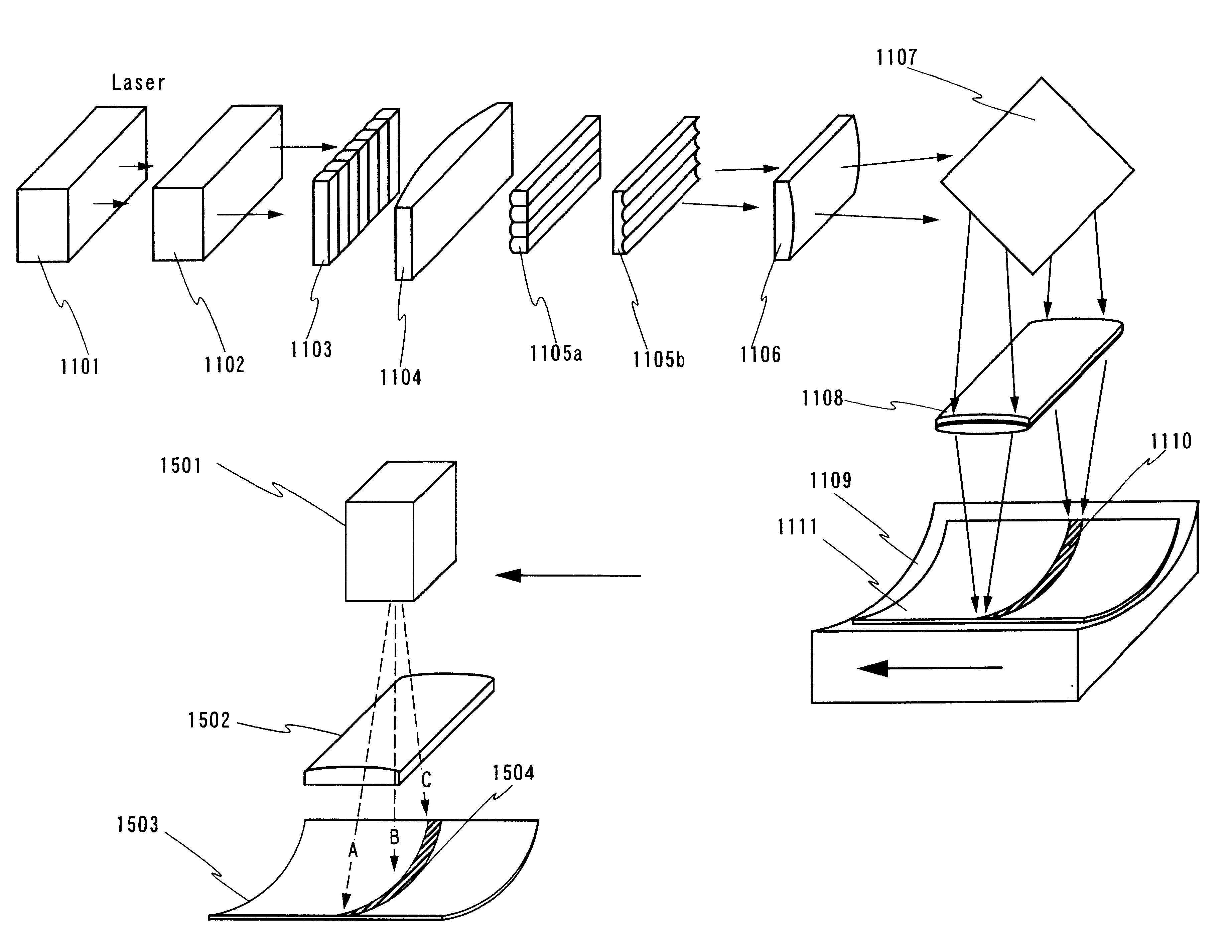
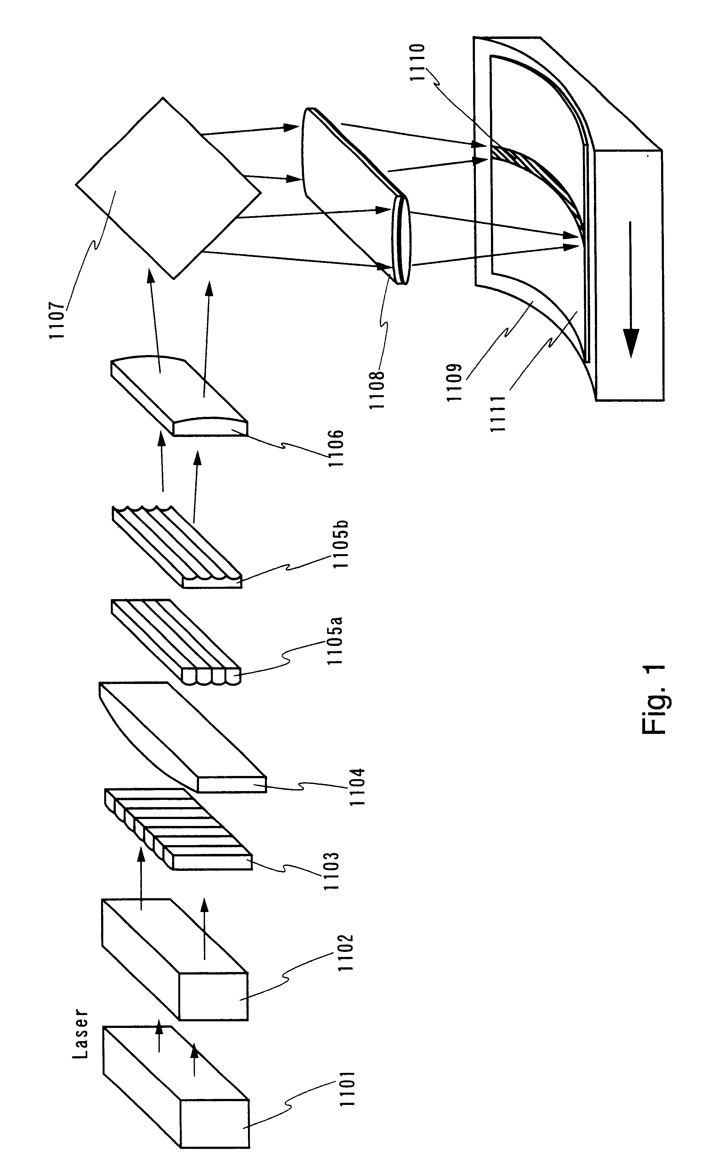
An embodiment of the present invention is explained using FIG. 1.

First, a 1000 mm.times.1200 mm.times.0.7 mm glass substrate is prepared. An insulating film is formed on one surface of the glass substrate by a known method (such as sputtering, plasma CVD, or reduced pressure CVD). Substrates made from glass such as barium borosilicate glass or aluminum borosilicate glass can be given as examples of the glass substrate. The insulating film may be formed using a silicon oxide film or the like, with a film thickness on the order of 200 nm. The insulating film functions as a blocking layer such that substances such as alkaline metal harmful to a semiconductor device do not incur upon the amorphous silicon film from the glass substrate. Note that quartz substrates, silicon substrates, plastic substrates, metallic substrates, stainless steel substrates, flexible substrates, and the like can also be used in addition to glass substrates. Further, flexible substrates having a fil...

embodiment 2

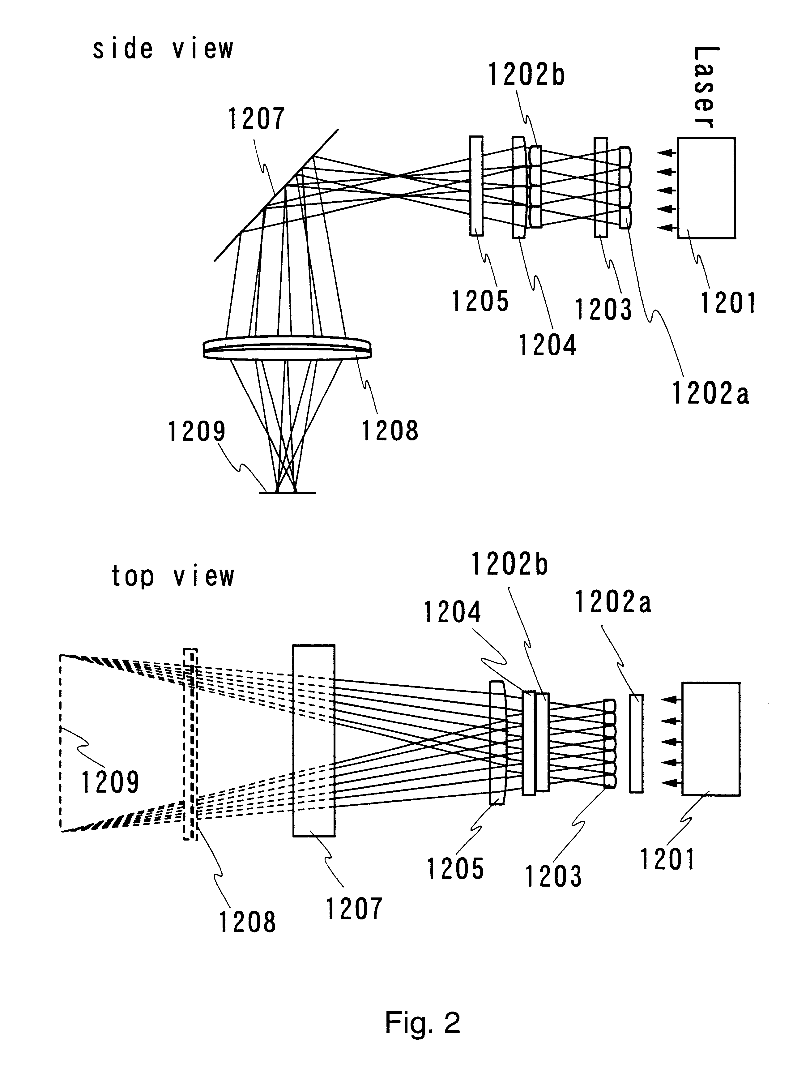
The energy distribution of laser beams in an irradiation surface are compared in embodiment 2 for cases in which the present invention is applied, and cases in which the present invention is not applied.

It is understood from Eq. (1)

(1)L=d.multidot.f2 / f1 Eq.(1)

that f2 / f1 is increased in order to make the length L in the longitudinal direction of a linear shape laser beam longer. (See FIG. 3 for each variable) It is also possible to make the width d of cylindrical lenses contained in a cylindrical lens array larger. This is not preferable, however, because the number of laser beam divisions is reduced, and therefore the uniformity of the energy distribution of the linear shape beam is damaged. Further, L becomes larger if f2 is increased, but the distance between the lens and an irradiation surface increases, and therefore the footprint becomes larger, which is uneconomical. Consequently, it can be understood that it is most preferable to reduce f1 in order to increase the length L in...

embodiment 3

An example is given in embodiment 3 of an optical system that differs from the optical systems discussed in embodiment 1 and embodiment 2. Specifically, an explanation is made regarding just how much curvature must be provided to a semiconductor film when the length of a linear shape beam is changed.

The length of the linear shape beam can be changed in the optical system shown in FIG. 1 by changing the focal distance of the cylindrical lens array 1103. An example of specific numerical values is as follows: if the length of the linear shape beam is 300 mm, the radius of curvature of the cylindrical lens array 1103 may be set to 14 mm, and if the length of the linear shape beam is 600 mm, then the radius of curvature may be set to 7 mm. In other words, it can be considered that there is an inversely proportional relationship between the radius of curvature and the linear beam length.

Simulation results for the energy distribution of a linear shape beam on an irradiation surface when th...


PUM

PropertyMeasurementUnit
melting point temperatureaaaaaaaaaa
lengthaaaaaaaaaa
widthaaaaaaaaaa

Abstract

As the output of laser oscillators become higher, it becomes necessary to develop a longer linear shape beam for a process of laser annealing of a semiconductor film. However, if the length of the linear shape beam is from 300 to 1000 mm, or greater, then the optical path length of an optical system for forming the linear shape beam becomes very long, thereby increasing its footprint size. The present invention shortens the optical path length. In order to make the optical path length of the optical system as short as possible, and to increase only the length of the linear shape beam, curvature may be given to the semiconductor film in the longitudinal direction of the linear shape beam. For example, if the size of the linear shape beam is taken as 1 mx0.4 mm, then it is necessary for the optical path length of the optical system to be on the order of 10 m. If, however, the semiconductor film is given curvature with a radius of curvature of 40,000 mm, then the optical path length of the optical system can be halved to approximately 5 m, and a linear shape beam having an extremely uniform energy distribution can be obtained.

Description

1. Field of the InventionThe present invention relates to a stage for specifying a shape of an irradiation surface onto which a laser beam is irradiated. Further, the present invention relates to a laser irradiation apparatus in which energy distribution of a laser beam is made uniform over a certain specific region. The present invention also relates to a method of making an energy distribution uniform, and to an optical system to realize the uniformity. Furthermore, the present invention relates to a method of making the energy distribution of a laser beam uniform over a certain specified region, and to a method of annealing a semiconductor film using the laser beam (the method is hereafter referred to as "laser annealing"). The present invention also relates to a method of manufacturing a semiconductor device, the semiconductor device having circuits structured by thin film transistors (hereafter referred to as "TFTs"), which includes a laser annealing process. For example, elect...

Claims


Application Information

Patent Timeline
Patent Type & Authority Patents(United States)
IPC IPC(8): B23K26/073B23K26/06G02B27/09H01L27/12H01L21/70H01L21/84H01S5/40H01S5/00H01L21/77H01L29/786
CPCG02B27/0961G02B27/0966G02B27/0977H01L27/12B23K26/0604B23K26/0738G02B27/09G02B27/0927G02B19/0052G02B19/0014H01L27/1285H01L29/78681H01S5/005H01S5/4012H01S5/4025B23K2201/40B23K2101/40
Inventor TANAKA, KOICHIRO
Owner SEMICON ENERGY LAB CO LTD
Why Eureka
Try Eureka