Flash memory device and a fabrication process thereof, method of forming a dielectric film

a technology of flash memory and fabrication process, which is applied in the direction of solid-state devices, solid-state diffusion coatings, coatings, etc., can solve the problems of erroneous erasing, large substrate current, and degradation of device performan

Inactive Publication Date: 2005-01-25
FOUND FOR ADVANCEMENT OF INT SCI
View PDF17 Cites 6 Cited by
  • Summary
  • Abstract
  • Description
  • Claims
  • Application Information

AI Technical Summary

Benefits of technology

Another and more specific object of the present invention is to provide a high-performance flash memory device having a high-quality insulation film that is formed at a low temperature process, the thickness of the tunneling gate insulation film or the thickness of the insulation film between the floating gate and the control gate can be reduced successfully without causing the problem of leakage current, and enabling writing and erasing at low voltage.
According to the present invention, it becomes possible to nitride the surface of the first electrode at low temperature by conducting the nitridation in the plasma of Ar or Kr in which the hydrogen nitride radicals NH* are formed efficiently.

Problems solved by technology

Such a conventional flash memory device, on the other hand, requires a high voltage at the time of writing or erasing of information, while the use of such a high voltage tends to cause a large substrate current.
The large substrate current, in turn, causes the problem of deterioration of the tunneling insulation film and hence the degradation of device performance.
Further, the use of such a high voltage limits the number of times rewriting of information can be made in a flash memory device and also causes the problem of erroneous erasing.
In the conventional art of film formation, there has been a problem, when a high-temperature process such as thermal oxidation process is used in the process of forming an oxide film such as the insulation film 1705 on the floating gate 1704, in that the quality of the interface between the polysilicon gate 1704 and the oxide film tends to become poor due to the thermal budget effect, etc.
However, it has been difficult to form a high-quality oxide film according to such a low-temperature process.
However, the use of large thickness for the insulation films 1705, 1706 and 1707 in these conventional flash memory devices has caused the problem in that it is necessary to use a large writing voltage and also a large erasing voltage.

Method used


Image

  • Flash memory device and a fabrication process thereof, method of forming a dielectric film
  • Flash memory device and a fabrication process thereof, method of forming a dielectric film
  • Flash memory device and a fabrication process thereof, method of forming a dielectric film

Examples


first embodiment

First, low temperature oxide film formation using plasma will be described.

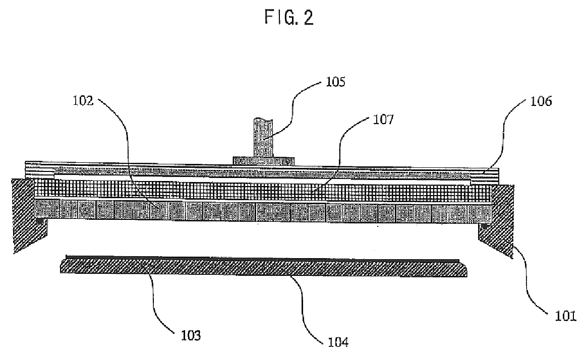
FIG. 2 is a cross sectional diagram showing the construction of an exemplary microwave plasma processing apparatus used in the present invention for realizing the oxidation process, wherein the microwave plasma processing apparatus uses a radial line slot antenna (see WO98 / 33362). The novel feature of the present embodiment is to use Kr as the plasma excitation gas at the time of forming the oxide film.

Referring to FIG. 2, the microwave plasma processing apparatus includes a vacuum vessel (processing chamber) 101 accommodating therein a stage 104 on which a substrate 103 to be processed is supported. The processing chamber 101 is evacuated to a vacuum state, and a Kr gas and an O2 gas are introduced from a shower plate 102 formed at a part of the wall of the processing chamber 101 such the pressure inside the processing chamber is set to about 1 Torr (about 133 Pa). Further, a disk-shaped substrate such as a ...

second embodiment

Next, the process of forming a nitride film at a low temperature by using high-density microwave plasma will be described.

In the formation of the nitride film, the same apparatus as the one explained with reference to FIG. 2 is used, except that Ar or Kr is used for the plasma excitation gas at the time of forming the nitride film.

Thus, the vacuum vessel (processing chamber) 101 is evacuated to a high vacuum state first, and the pressure inside the processing chamber 101 is then set to about 100 mTorr (about 13 Pa) by introducing an Ar gas and a NH3 gas via the shower plate 102, and the like. Further, a disk-shaped substrate such as a silicon wafer is placed on the stage 104 as the substrate 103 and the substrate temperature is set to about 500° C. As long as the substrate temperature is in the range of 400-500° C., almost the same results are obtained.

Next, a microwave of 2.45 GHz is introduced into the processing chamber from the coaxial waveguide 105 via the radial line slot ante...

third embodiment

The foregoing method of forming oxide film or nitride film is applicable also to the oxidation or nitridation of polysilicon. Thus, the present invention enables formation of a high-quality oxide film or nitride film on polysilicon.

Hereinafter, the method of forming a dielectric film on a polysilicon film according to a third embodiment of the present invention will be described with reference to FIGS. 11A and 11B.

Referring to FIG. 11A, a polysilicon film 203 is deposited on a silicon substrate 201 covered by an insulation film 202. By exposing the polysilicon film 203 to the high-density mixed gas plasma of Kr or Ar and oxygen in the processing vessel 101 of the microwave plasma processing apparatus of FIG. 2 in the step of FIG. 11B, a silicon oxide film 204 having a high film quality is obtained on the surface of the polysilicon film 203, wherein the silicon oxide film 204 thus formed is characterized by small surface state density and small leakage current.

In the step of FIG. 11B...


PUM

PropertyMeasurementUnit
electron densityaaaaaaaaaa
thicknessaaaaaaaaaa
thicknessaaaaaaaaaa

Abstract

A fabrication process of a flash memory device includes microwave excitation of high-density plasma in a mixed gas of Kr and an oxidizing gas or a nitriding gas. The resultant atomic state oxygen O* or hydrogen nitride radicals NH* are used for nitridation or oxidation of a polysilicon electrode surface. It is also disclosed the method of forming an oxide film and a nitride film on a polysilicon film according to such a plasma processing.

Description

TECHNICAL FIELDThe present invention generally relates to semiconductor devices and a fabrication process thereof. More particularly, the present invention relates to a method of forming a dielectric film and fabrication process of a non-volatile semiconductor memory device capable of rewriting information electrically, including a flash memory device.There are various volatile memory devices such as DRAMs and SRAMs. Further, there are non-volatile memory devices such as a mask ROM, PROM, EPROM, EEPROM, and the like. Particularly, a flash memory device is an EEPROM having a single transistor for one memory cell and has an advantageous feature of small cell size, large storage capacity and low power consumption. Thus, intensive efforts are being made on the improvement of flash memory devices. In order that a flash memory device can be used stably over a long interval of time with low voltage, it is essential to use a uniform insulation film having high film quality.BACKGROUND ARTFir...

Claims


Application Information

Patent Timeline
Patent Type & Authority Patents(United States)
IPC IPC(8): H01L21/02H01L21/336H01L21/31C23C8/02C23C8/36H01L21/3105H01L21/314H01L21/316H01L21/318H01L21/8238H01L21/8247H01L27/105H01L27/115H01L29/423H01L29/792
CPCC23C8/02H01L29/42324H01L21/0217H01L21/02238H01L21/02247H01L21/02252H01L21/02323H01L21/02329H01L21/0234H01L21/3105H01L21/3144H01L21/31612H01L21/31637H01L21/31641H01L21/31662H01L21/3185H01L27/105H01L27/115H01L27/11521H01L27/11526H01L27/11546C23C8/36H10B41/40H10B41/49H10B69/00H10B41/30H01L21/31
Inventor OHMISUGAWA, SHIGETOSHI
Owner FOUND FOR ADVANCEMENT OF INT SCI
Why Eureka
Try Eureka