Organic thin film transistor (OTFT)

a thin film transistor and organic technology, applied in the direction of thermoelectric devices, bulk negative resistance effect devices, radiation controlled devices, etc., can solve the problems of increasing the leakage current between the gate electrode and the source electrode, comparatively difficult to deal with the fine finish of this kind of device, and poor insulatibity of materials with high dielectric constants, so as to achieve effective reduction of leakage current and high performan

Inactive Publication Date: 2005-01-25
CHANGCHUN FULEBO DISPLAY TECH
View PDF3 Cites 9 Cited by
  • Summary
  • Abstract
  • Description
  • Claims
  • Application Information

AI Technical Summary

Benefits of technology

The present invention aims at providing a high performance OTFT device which can effectively reduce the leakage current between the gate electrode and the source electrode, between the gate electrode and the drain electrode.

Problems solved by technology

Because the organic semiconductor materials are sensitive to some chemical solvents generally used in the traditional process of photolithography, it is comparatively difficult to deal with this kind of device's fine finish.
Unfortunately, all the two methods increase the leakage current between the gate electrode and the source electrode, between the gate electrode and the drain electrode.
The main reason is that the material with high dielectric constant is poor in insulatibity.
However, neither of the above two methods can solve the above-mentioned problems.

Method used


Image

  • Organic thin film transistor (OTFT)
  • Organic thin film transistor (OTFT)
  • Organic thin film transistor (OTFT)

Examples


example 1

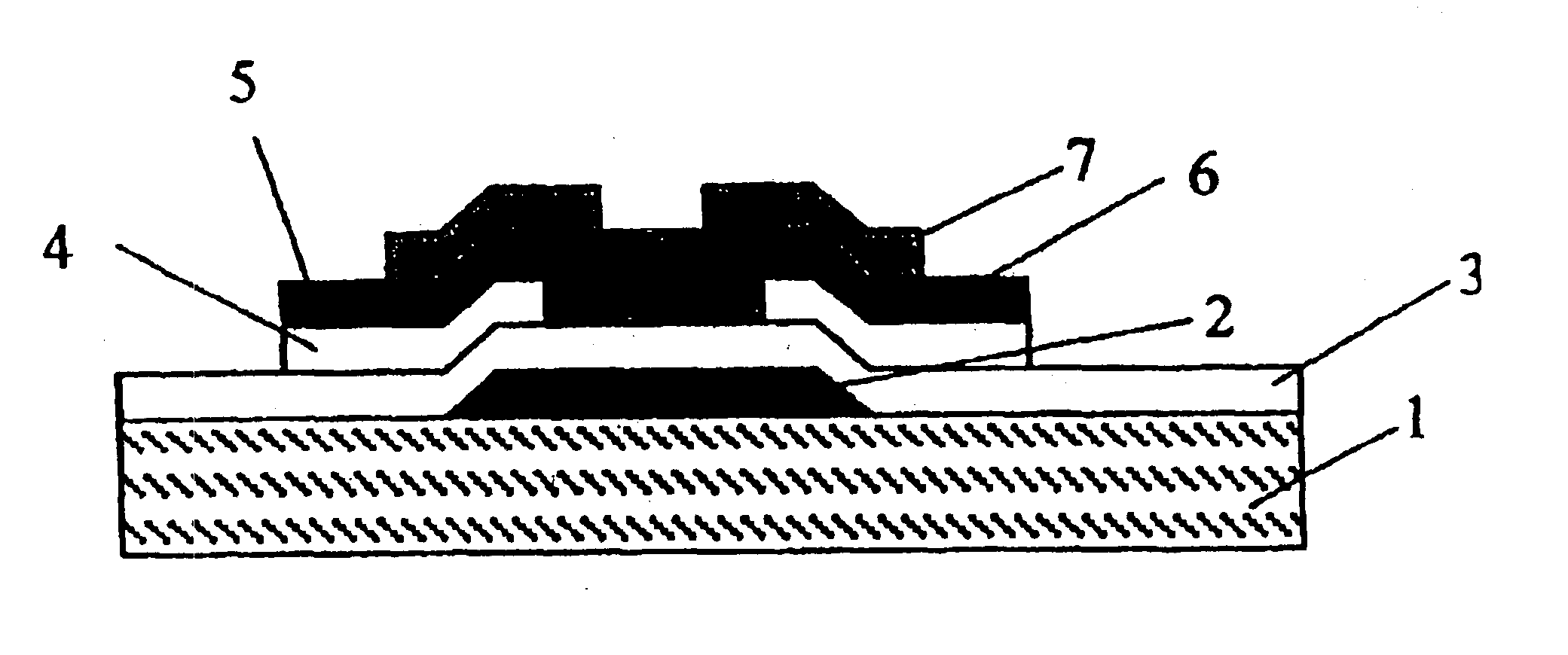
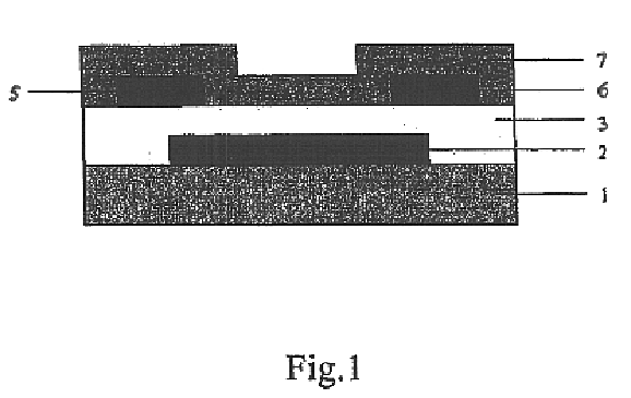
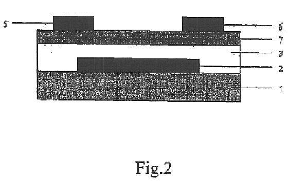
As shown in FIG. 6, a layer of metal Ta was plated on a 7059 glass substrate (1) by the RF magnetism controlled sputtering method. The sputtering conditions were as follows: a background vacuum of 2×10⁻³ Pa; a Ar pressure of 1 Pa; a RF power of 500 W; and a substrate temperature of 100 centigrade. Then the layer of metal Ta was shaped into the gate electrode (2) by the photolithography method. A layer of Ta2O5 400 nm in thickness and a layer of SiO2 300 nm in thickness were continuously sputtered on the gate electrode respectively as the gate insulation layer (3) and the second insulation layer (4) by the DC magnetism controlled sputtering method. The reactive sputtering conditions were as follows: a background vacuum of 2×10⁻³ Pa; a O2 pressure of 0.9 Pa; a DC power of 500 W; and a substrate temperature of 100 centigrade. Next, the photo-resist was coated, exposed and developed. Then a layer of Au 100 nm in thickness was formed by the method of heat evaporation at a vacuum of 10−5 ...

example 2

As shown in FIG. 6, a layer of alloy MoW was plated on the flexible plastic substrate (1) by co-sputtering target Mo and W using the RF magnetism controlled sputtering method. The sputtering conditions are as follows: a background vacuum of 2×10⁻³ Pa; a Ar pressure of 1 Pa; a RF power of 500 W; and a substrate temperature of 100 centigrade. Then the layer of metal Ta was shaped into the gate electrode (2) by the photolithography method. A layer of Ta2O5 500 nm in thickness was sputtered on the gate electrode as the gate insulation layer (3) by the DC magnetism controlled sputtering method. The reactive sputtering conditions were as follows: a background vacuum of 2×10⁻³ Pa; a O2 pressure of 0.9 Pa; a DC power of 500 W; and a substrate temperature of 100 centigrade. Subsequently, a layer of poly(methyl methacrylate) (PMMA) 300 nm in thickness was spin coated as the second insulation layer (4). Next, the photo-resist was coated, exposed and developed. Then a layer of silver (Ag) 100 n...

example 3

As shown in FIG. 6, a layer of metal Cr was plated on the flexible plastic substrate (1) by sputtering target Cr using the RF magnetism controlled sputtering method. The sputtering conditions are as follows: a background vacuum of 2×10⁻³ Pa; a Ar pressure of 1 Pa; a RF power of 500 W; and a substrate temperature of 100 centigrade. Then the layer of metal Ta was shaped into the gate electrode (2) by the photolithography method. A layer of TiO2 500 nm in thickness was sputtered on the gate electrode as the gate insulation layer (3) by the DC magnetism controlled sputtering method. The reactive sputtering conditions were as follows: a background vacuum of 2×10⁻³ Pa; a O2 pressure of 0.9 Pa; a DC power of 500 W; and a substrate temperature of 100 centigrade. Subsequently, a layer of polyimide 300 nm in thickness was spin coated as the second insulation layer (4). Next, a layer of silver (Al) 100 nm in thickness was formed by the method of heat evaporation at a vacuum of 10−5 Pa. Then, t...


PUM


Abstract

The present invention relates to an organic thin film transistor (OTFT) comprising: a substrate (1), a gate electrode (2) formed on the substrate (1), a gate insulation layer formed on the gate electrode, a source electrode (5) and a drain electrode (6) formed on the gate insulation layer including a first insulation layer (3) and a second insulation layer (4) with different dielectric constants, and an active layer (7) which overlays the source electrode (5) and the drain electrode (6). Without adding the conventional complicated processes like photolithography but adding two simple processes of spin coating or vaporously coating the second insulation film and self-aligned dry RIE, the present invention not only can improve the carrier's injection property so as to improve the OTFT device's properties, but also can block the leakage current of the gate insulation layer and reduce the device's parasitic capacitance. Therefore, the material with high dielectric constant can be used as the insulation layer to increase the channel capacitance so as to reduce threshold voltage of the device and reduce the adverse effect of the leakage between the source and gate electrodes, the gate and drain electrodes.

Description

BACKGROUND OF THE INVENTION1. Field of the InventionThe present invention relates to a kind of organic thin film transistor (to be abbreviated as OTFT hereinafter) and a manufacturing method thereof.2. Description of the Related ArtIn recent years, the performances of the OTFT have been continuously improved. The carrier mobility of some transistors made of such organic materials as Pentacene, Oligothiophene, Tetracene and so on is over 1 cm2 / V.s, therefore, these transistors are potential in such practical applications as active matrix display, flexural integrated circuit (to be abbreviated as IC hereinafter) and so on. Because the organic semiconductor materials are sensitive to some chemical solvents generally used in the traditional process of photolithography, it is comparatively difficult to deal with this kind of device's fine finish. At present, the method of setting the organic semiconductor layer above the source / drain electrode (generally referred to bottom electrode OTFT...

Claims


Application Information

Patent Timeline
Patent Type & Authority Patents(United States)
IPC IPC(8): H01L21/02H01L21/316H01L51/30H01L51/05H01L29/76H01L35/24H01L47/00H01L51/00
CPCH01L51/0545H01L51/0516H01L21/31604H01L21/31691H01L51/0078H01L28/56H10K85/311H10K10/468H10K10/466H01L21/02263H01L21/02197H10K10/474
Inventor YAN, DONGHANGYUAN, JIANFENG
Owner CHANGCHUN FULEBO DISPLAY TECH
Why Eureka
Try Eureka