

Providing an emission-protecting layer in an OLED device
- Summary
- Abstract
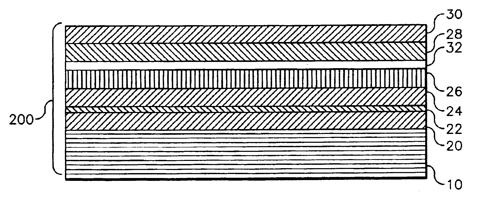
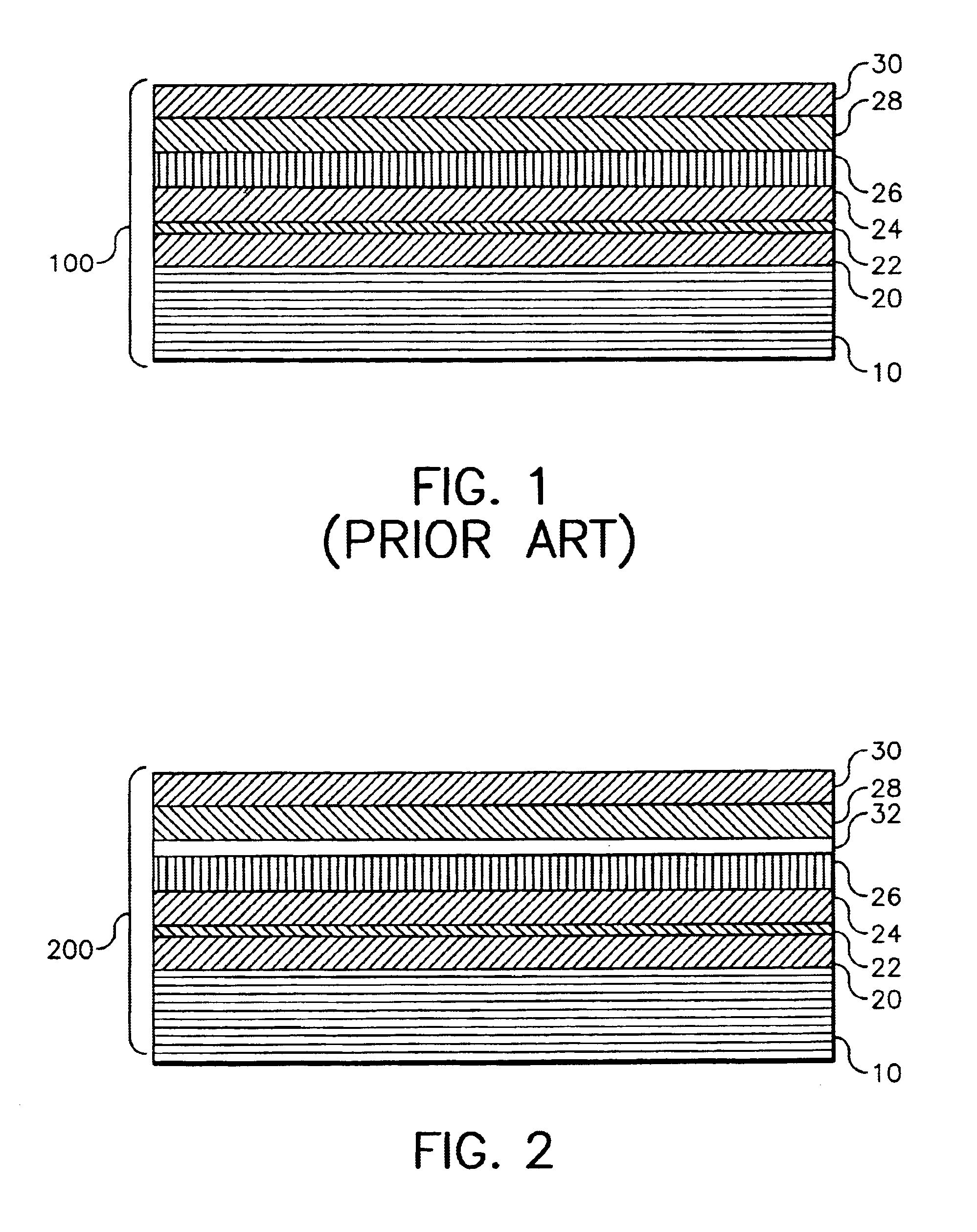
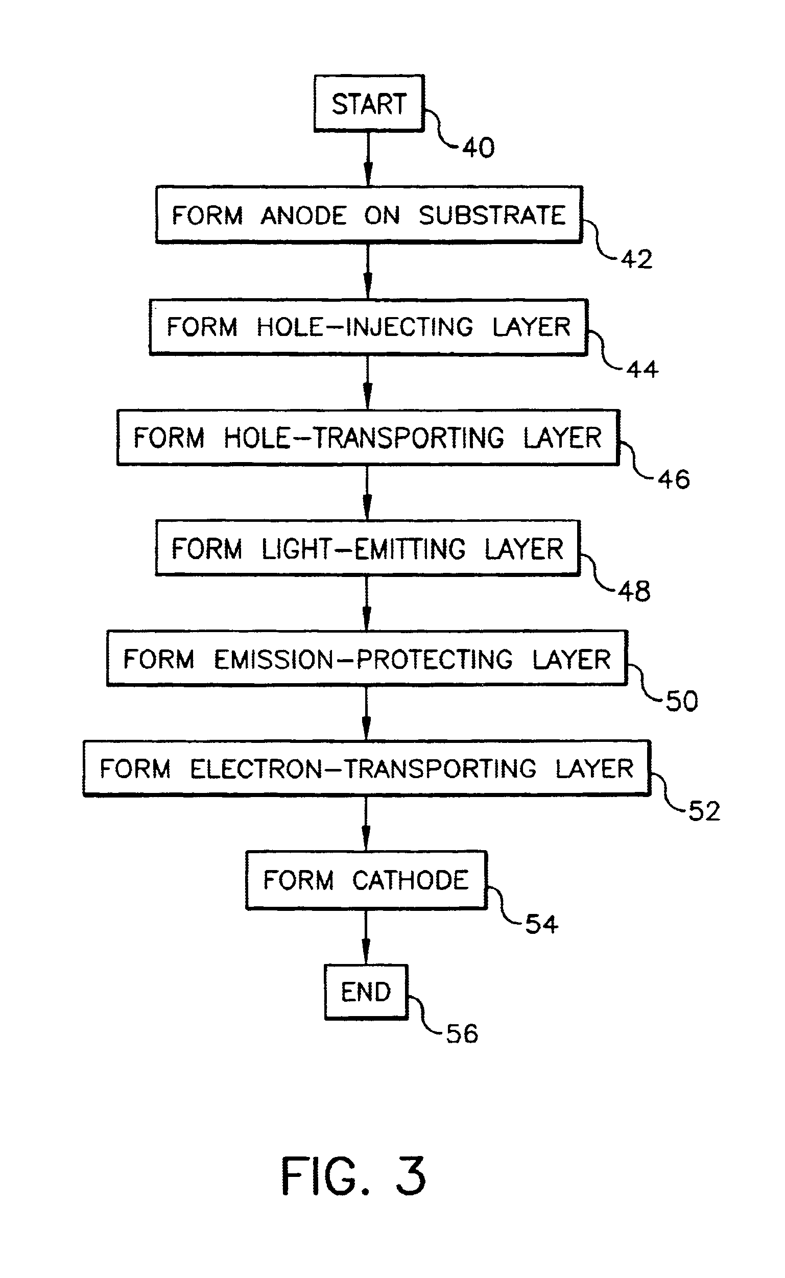
- Description
- Claims
- Application Information
AI Technical Summary
Benefits of technology
Problems solved by technology
Method used
Image

Examples
example 1 (
Inventive Example)
An OLED device with an emission-protecting layer satisfying the requirements of the invention was constructed in the following manner:1. A clean glass substrate was vacuum-deposited with indium tin oxide (ITO) to form a transparent electrode of 34 nm thickness. The sheet resistance of the ITO layer is about 60 Ω / square.2. The above-prepared ITO surface was treated with a plasma oxygen etch, followed by plasma deposition of a 1.0 nm layer of a fluorocarbon polymer (CFx) as described in U.S. Pat. No. 6,208,075.3. The above-prepared substrate was further treated by vacuum-depositing under a vacuum of approximately 10−6 Torr a 75 nm HTL of 4,4′-bis[N-(1-naphthyl)-N-phenylamino]biphenyl (NPB) from a heated boat source.4. A coating of 20 nm of tris(8-quinolinolato)aluminum (III) (Alq) as a LEL was vacuum-deposited onto the HTL at a coating station that included a heated boat source.5. A coating of 2 nm 2-(1,1-dimethyethyl)-9,10-bis(2-naphthalenyl)anthracene (TBADN) as an...
example 4 (
Inventive Example)
An OLED device with an emission-protecting layer satisfying the requirements of the invention was constructed in the following manner:1. A clean glass substrate was vacuum-deposited with indium tin oxide (ITO) to form a transparent electrode of 30 nm thickness. The sheet resistance of the ITO layer is about 100 Ω / square.2. The above-prepared ITO surface was treated with a plasma oxygen etch, followed by plasma deposition of a 1.0 nm layer of a fluorocarbon polymer (CFx) as described in U.S. Pat. No. 6,208,075.3. The above-prepared substrate was further treated by vacuum-depositing under a vacuum of approximately 10−6 Torr a 75 nm HTL of 4,4′-bis[N-(1-naphthyl)-N-phenylamino]biphenyl (NPB) from a heated boat source.4. A coating of 20 nm of tris(8-quinolinolato)aluminum (III) (Alq) as a LEL was vacuum-deposited onto the HTL at a coating station that included a heated boat source.5. A coating of 2 nm bis(2-methyl-8-quinolinolato)(4-phenylphenolato)aluminum (B-Alq) as ...
example 7 (
Inventive Example)
An OLED device was constructed in the manner described in Example 1, except that Step 6 was changed as:6. Evaporate a 0.1 nm thick film of 4-(dicyanomethylene)-2-t-butyl-6-(1,1,7,7,-tetramethyljulolidyl-9-enyl)-4H-pyran (DCJTB) from a coating station that included a heated boat source in order to create an environment having DCJTB molecules in the vacuum with a partial pressure of about 10−6 Torr. The DCJTB molecules were prevented from directly depositing on the surface of the organic layer. This was a simulation of the fabrication process for full color displays. The evaporation process of DCJTB was finished within about 10 min.
The initial device performance was tested by applying a constant current of 20 mA / cm2 across the electrodes at room temperature. The driving voltage was 8.3 V, the luminance was 628 cd / m2, and the luminous efficiency was 3.1 cd / A. After the initial testing, the device was operated at 20 mA / cm2 in a 70° C. oven for stability testing. There ...
PUM
| Property | Measurement | Unit |
|---|---|---|
| Thickness | aaaaa | aaaaa |
| Thickness | aaaaa | aaaaa |
| Thickness | aaaaa | aaaaa |
Abstract
Description
Claims
Application Information