Laminate having mono-crystal oxide conductive member on silicon substrate, actuator using such laminate, ink jet head and method for manufacturing such head

a technology of monocrystal oxide and conductive member, which is applied in the direction of ink jet head manufacturing, crystal growth process, ink jet head, etc., can solve the problems of difficult to obtain good crystallization of piezoelectric film formed on the sro, the firm formation of sro on the silicon substrate is apt to be worsened, and the cost of mbe method is required. , to achieve the effect of high density, high frequency and great dischar

Inactive Publication Date: 2005-02-15
CANON KK
View PDF12 Cites 42 Cited by
  • Summary
  • Abstract
  • Description
  • Claims
  • Application Information

AI Technical Summary

Benefits of technology

In the manufacturing method for manufacturing the actuator and ink jet head according to the present invention, since the piezoelectric material and / or electrostrictive element are mono-crystal or uni-orientation similar to the mono-crystal oxide conductive member, an actuator and an ink jet head in which discharge ports are arranged with high density and have great discharging forces and which is not deteriorated due to peeling and which can cope with high frequency can be provided. The present invention has an advantage that external stress during the film formation can be removed by performing the epitaxial growth of the piezoelectric element on the mono-crystal oxide conductive member transferred to the silicon substrate. As a result, a factor for obstructing the driving is removed, and, thus, rapid progress is achieved. Further, deterioration of performance of the piezoelectric element caused by the peeling at the interface between the mono-crystal piezoelectric element and silicon or between the mono-crystal piezoelectric element and SiO2 can be prevented.

Problems solved by technology

However, in the above proposal, SRO is multi-crystal, and there is no description regarding a method for utilizing a piezoelectric element having good orientation property or mono-crystal.
However, in order to achieve the epitaxial growth, an expensive method such as an MBE method is required.
In this method, there were problems that crystallization of the SRO firm-formed on the silicon is apt to be worsened since the unnecessary plural layers are used and that good crystallization of the piezoelectric film formed on the SRO is hard to be obtained.
Further, if mono-crystal bodies formed by a Bernoulli method are stuck together and polished, a film thickness is limited and a uniform film cannot be obtained, and, since the film itself cannot be used as an oscillating plate, it cannot be used as an electrode of an actuator of a micro-machine, which requires a thin film thickness.
Furthermore, if an actuator and an ink jet head using oxide conductive material directly formed on the silicon as the electrode are driven, peeling at an interface between the oxide conductive material and the silicon is apt to occur thereby to worsen endurance.

Method used


Image

  • Laminate having mono-crystal oxide conductive member on silicon substrate, actuator using such laminate, ink jet head and method for manufacturing such head
  • Laminate having mono-crystal oxide conductive member on silicon substrate, actuator using such laminate, ink jet head and method for manufacturing such head
  • Laminate having mono-crystal oxide conductive member on silicon substrate, actuator using such laminate, ink jet head and method for manufacturing such head

Examples


embodiment 1

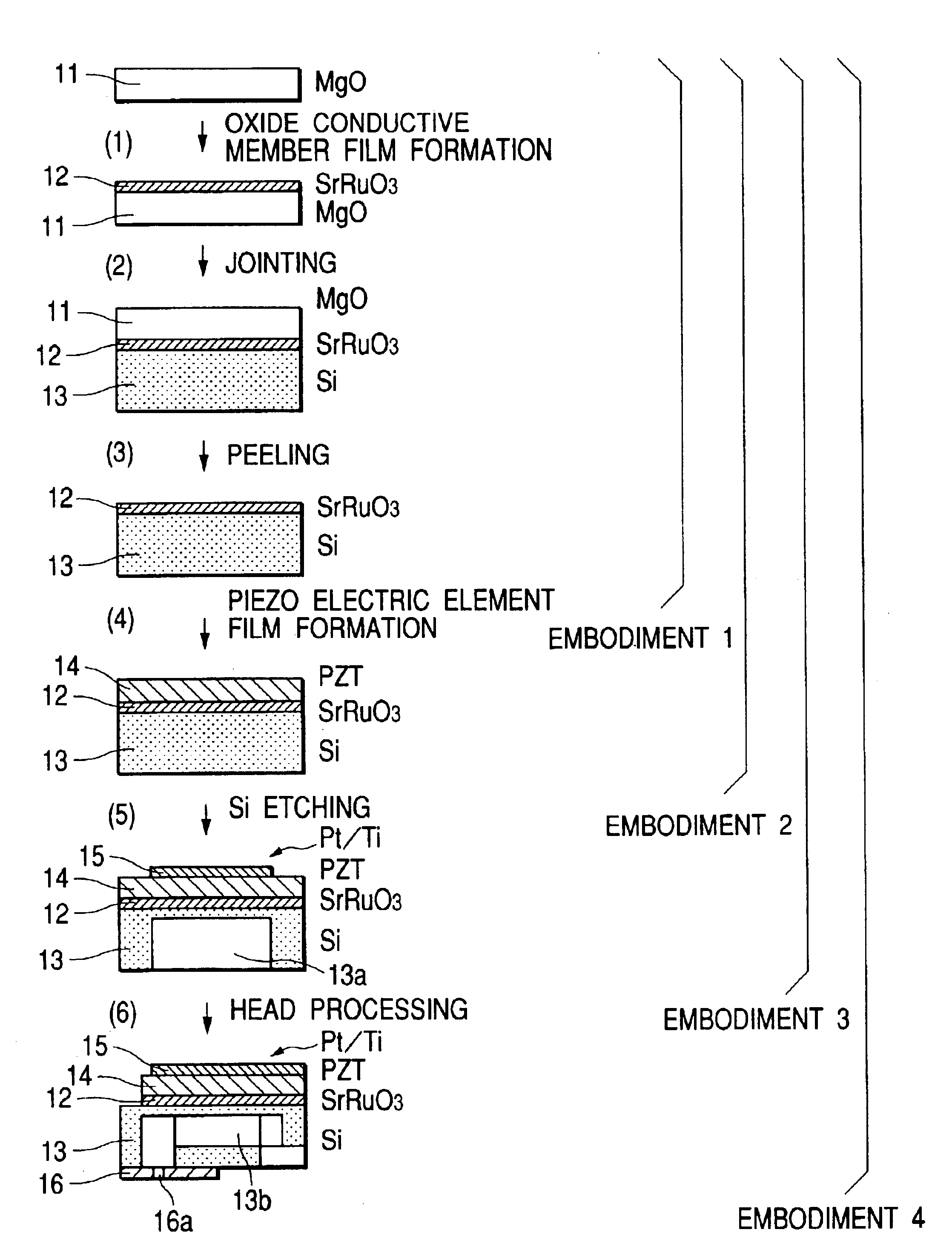
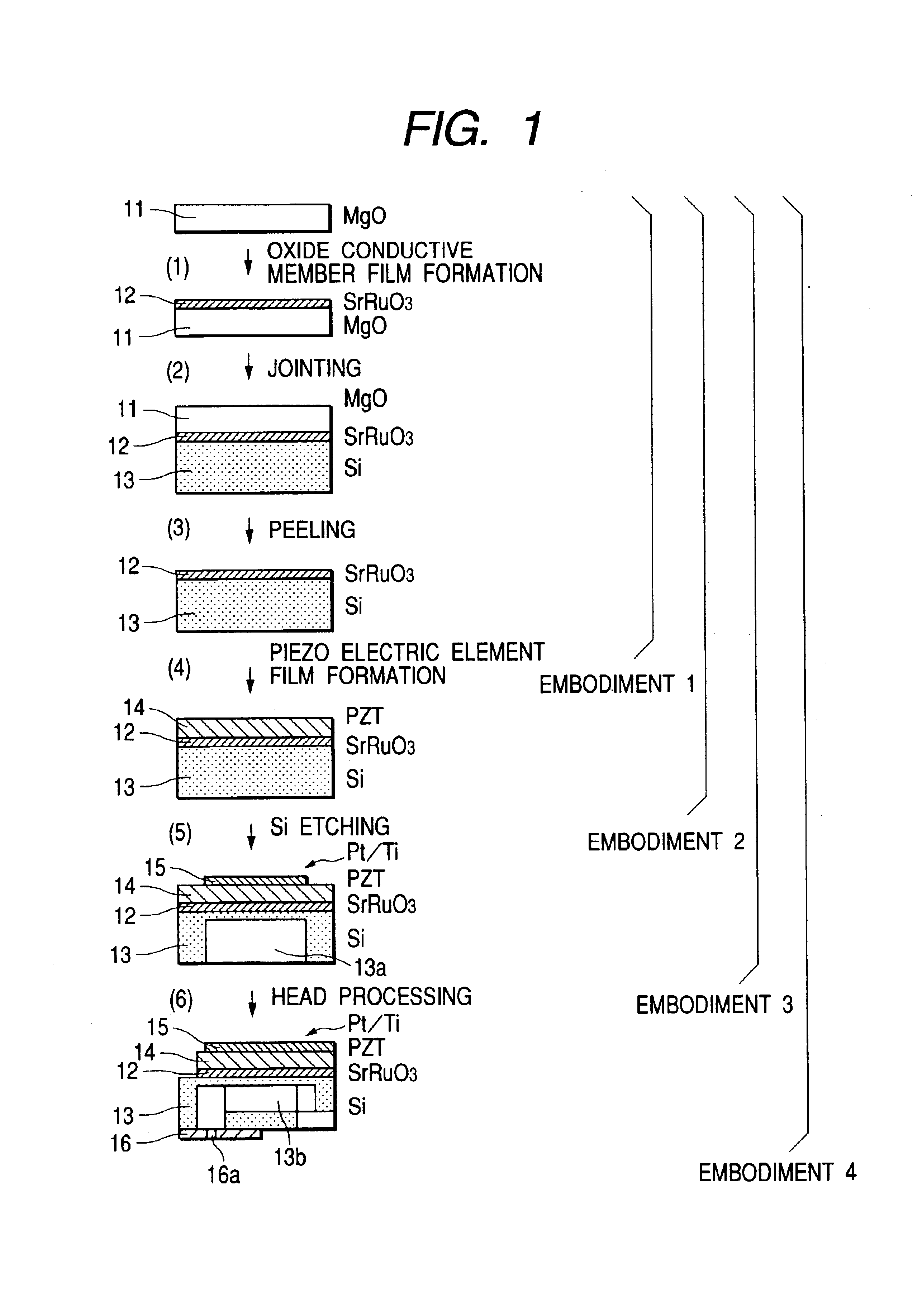
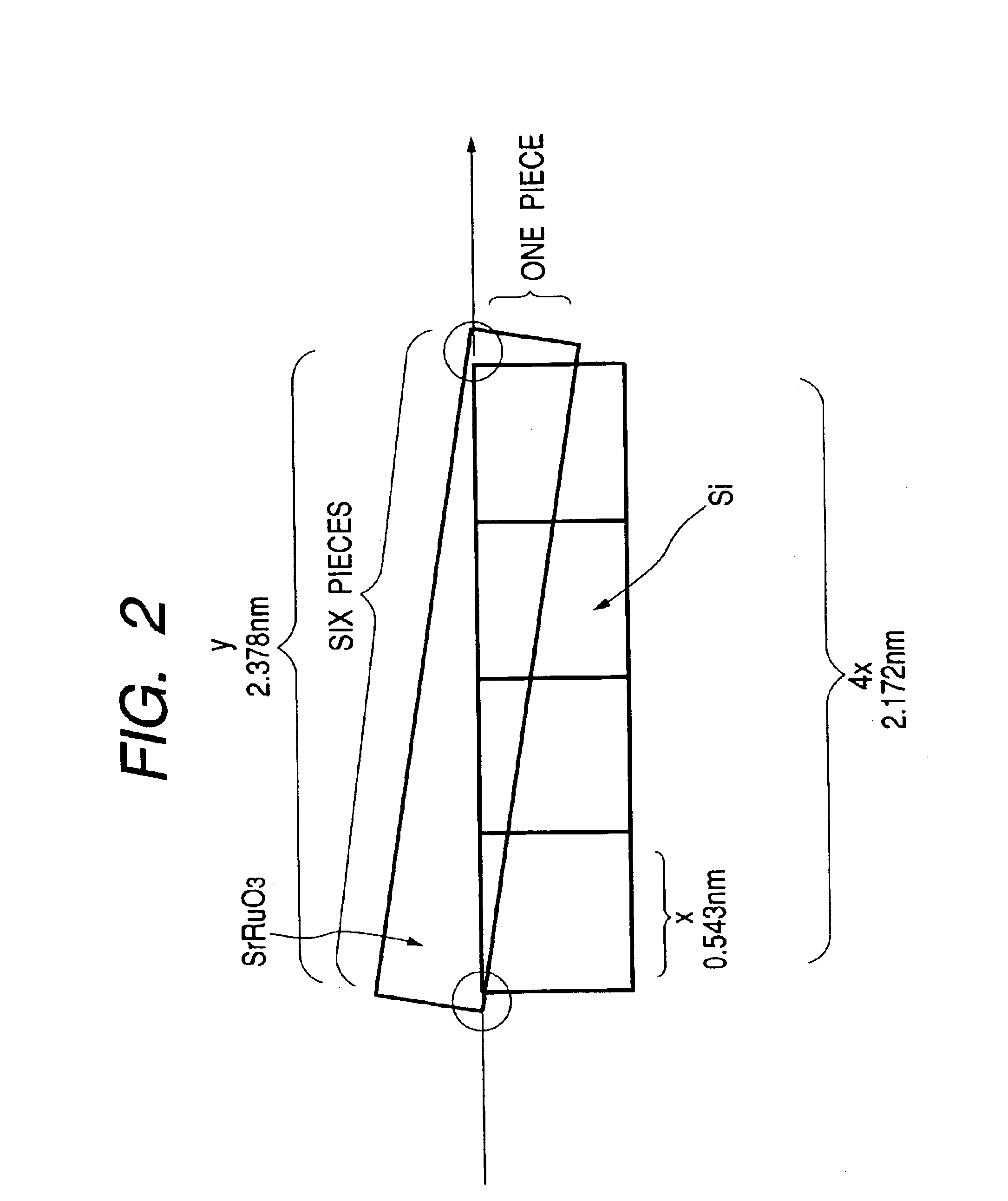
A flow chart of a method for manufacturing a mono-crystal oxide conductive member on a silicon substrate according to a first embodiment of the present invention is shown by (1) to (3) in FIG. 1.(1) Epitaxial growth of SrRuO3 as mono-crystal oxide conductive material 12 was performed on an MgO substrate (mono-crystal production substrate 11).(2) The mono-crystal oxide conductive member obtained in this way was jointed onto a silicon substrate 13 by a direct jointing method. (3) Then, MgO (mono-crystal production substrate 11) was peeled and removed by using an excimer laser (KrF laser; exposing energy=350 mJ / cm2). In this way, two kinds of mono-crystal oxide conductive member / silicon samples (sample 1 and sample 2) were produced. Regarding each of the mono-crystal oxide conductive member / silicon samples, a film thickness and surface roughness were measured by a surface step difference meter (α-STEP). As a result, the film thickness of SrRuO3 (mono-crystal oxide conductive member) wa...

embodiment 2

Next, an embodiment of a mono-crystal oxide conductive member on a silicon substrate according to a second embodiment of the present invention will be explained.

A flow chart of a method for manufacturing a piezoelectric element / mono-crystal oxide conductive member / silicon substrate according to a second embodiment of the present invention is shown by (1) to (4) in FIG. 1. Epitaxial growth of SrRuO3 as mono-crystal oxide conductive material 12 was performed on an MgO substrate (mono-crystal production substrate 11) by a spattering method while adequately heating the substrate. The mono-crystal oxide conductive member obtained in this way is jointed onto a silicon substrate 13. Then, MgO (mono-crystal production substrate 11) is peeled by using an excimer laser or an infrared laser and is removed, for example, by etching using heated concentrated phosphoric acid. Here, the mono-crystal production substrate 11 may be STO, MgAl2O4 or sapphire other than MgO. In this way, the mono-crysta...

embodiment 3

A flow chart for the manufacture of an actuator using the piezoelectric element / mono-crystal oxide conductive member / silicon substrate according to a third embodiment of the present invention is shown in FIG. 1. As shown in (5) of FIG. 1, an upper electrode 15 was provided on PZT 14 and a recess 13a was formed in the silicon substrate 13. A construction of an actuator according to the embodiment of the present invention in which a film is vibrated upwardly and downwardly by applying voltage is shown in FIG. 5. In FIG. 5, the reference numeral 1 denotes a substrate; 2 denotes a mono-crystal oxide conductive member; 3 denotes a piezoelectric element; and 4 denotes an upper electrode. A layer structure according to the illustrated embodiment is Pt / Ti (upper electrode) / PZT (mono-crystal piezoelectric element) / SrRuO3 (mono-crystal oxide conductive member) / silicon substrate. A film thickness of this actuator is Pt / Ti (upper electrode) (200 nm / 20 nm) / PZT (piezoelectric element) (3 μm) / SrRu...


PUM

PropertyMeasurementUnit
distanceaaaaaaaaaa
thicknessaaaaaaaaaa
distanceaaaaaaaaaa

Abstract

In a mono-crystal oxide conductive member on a silicon substrate, including an electrode material of a perovskite type piezoelectric element and an electrostrictive material and an oxide conductive material as a film formation substrate, a distance x between silicon atoms and a distance y between atoms of the mono-crystal oxide conductive member satisfy the following relationship: Z=mynx-1min0.05
(n and m are given positive integers, 1≦n≦5, 1≦m≦7 and nx≦3, my≦3).

Description

BACKGROUND OF THE INVENTION1. Field of the InventionThe present invention relates to a laminate having a mono-crystal oxide conductive member on a silicon substrate, an actuator using such a laminate, an ink jet head used in an ink jet recording apparatus, and a method for manufacturing such an ink jet head.2. Related Background ArtIn recent years, printers using an ink jet recording apparatus as a printing device for a personal computer and the like have widely been popularized because they have good printing performance and are easy to handle and are inexpensive. There are various types of ink jet recording apparatuses such as an ink jet recording apparatus of type in which a bubble is generated in ink by thermal energy and an ink droplet is discharged by a pressure wave caused by the bubble, an ink jet recording apparatus of type in which an ink droplet is sucked and discharged by an electrostatic force, an ink jet recording apparatus of type in which a pressure wave caused by an...

Claims


Application Information

Patent Timeline
Patent Type & Authority Patents(United States)
IPC IPC(8): B41J2/16H01L41/09H01L41/22H01L41/00H01L41/047B41J2/045B41J2/055B41J2/135B41J2/14C30B29/16H01L41/08H01L41/187H01L41/314
CPCB41J2/14233B41J2/161B41J2/1623B41J2/1628B41J2/1629B41J2/1634H01L41/0973B41J2/1643H01L41/314H01L41/319B41J2/1642B41J2202/03H01L41/0478H01L41/1876H10N30/878H10N30/2047H10N30/8554H10N30/074H10N30/079
Inventor MATSUDA, TAKANORI
Owner CANON KK
Why Eureka
Try Eureka