Semiconductor device and method for manufacturing the same

a semiconductor and film technology, applied in semiconductor devices, lighting and heating apparatus, burners, etc., can solve the problems of difficult to form insulating materials, unintentional etching of the base layer 602/b>, damage to the glass substrate, etc., and achieve excellent uniformity, high resistivity region, and low resistance of such a film

Inactive Publication Date: 2005-03-15
SEMICON ENERGY LAB CO LTD
View PDF168 Cites 149 Cited by
  • Summary
  • Abstract
  • Description
  • Claims
  • Application Information

AI Technical Summary

Benefits of technology

In accordance with the present invention, a surface of a gate electrode is oxidized and this oxide layer is used to define the high resistivity region. The oxide layer is formed, for example, by anodic oxidation. The use of the anodic oxidation to form the oxide layer is advantageous as compared with the anisotropic etching mentioned above because the thickness of the anodic oxide layer can be precisely controlled and can be formed as thin as 1000 Å or less and as thick as 5000 Å or more with an excellent uniformity.
Further, it is another feature of the present invention that there are two kinds of anodic oxide in the above mentioned anodic oxide layer. One is called a barrier type anodic oxide and the other is called a porous type anodic oxide. The porous anodic oxide layer can be formed when using an acid electrolyte. A pH of the electrolyte is lower than 2.0, for example, 0.8-1.1 in the case of using an oxalic acid aqueous solution. Because of the strong acidness, the metal film is dissolved during the anodization and the resultant anodic oxide becomes porous. The resistance of such a film is very low so that the thickness of the film can be easily increased. On the other hand, the barrier type anodic oxide is formed using a weaker acid or approximately neutral electrolyte. Since the metal is not dissolved, the resultant anodic oxide becomes dense and highly insulating. An appropriate range of pH of the electrolyte for forming the barrier type anodic oxide is higher than 2.0, preferably, higher than 3, for example, between 6.8 and 7.1.

Problems solved by technology

The foregoing process was achieved by copying the old LDD technique for a conventional semiconductor integrate circuit and this method has some disadvantages for a thin film process on a glass substrate as discussed below.
However, in the case of forming TFTs on a glass substrate, the high temperature of the heat annealing tends to damage the glass substrate.
Also, it is difficult to form the insulating material 609.
Accordingly, there is a danger that the base layer 602 is unintentionally etched and the substrate is exposed when etching the insulating film 608.
As a result, a production yield can not be increased because substrates for TFTs contain a lot of elements harmful for silicon semiconductors.
Further, it is difficult to control the thickness of the insulating material 609 accurately.
However, because of the use of a substrate having an insulating surface as is different from the use of a silicon substrate in a semiconductor integrated circuit, the delicate control of the plasma is difficult.
Therefore, the formation of the insulating material 609 is difficult.
Since the above HRD should be made as thin as possible, the above difficulty in precisely controlling the formation of the insulating material 609 makes it difficult to mass produce the TFT with a uniform quality.
Also, the necessity of performing the ion doping twice makes the process complicated.

Method used


Image

  • Semiconductor device and method for manufacturing the same
  • Semiconductor device and method for manufacturing the same
  • Semiconductor device and method for manufacturing the same

Examples


example 1

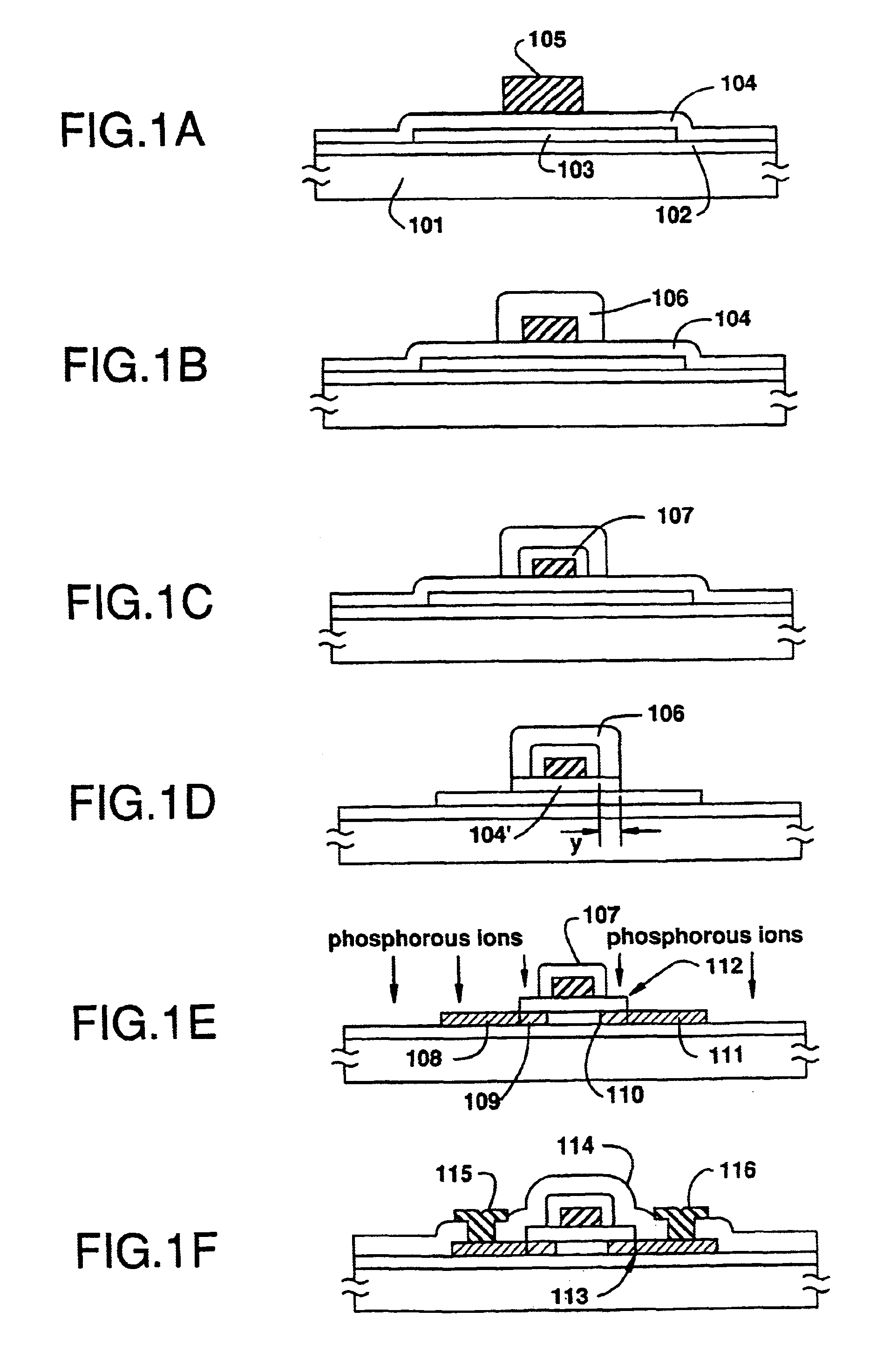
Referring again to FIGS. 1A-1F, a process of manufacturing a TFT will be discussed in more detail. A Corning 7059 glass substrate having a dimension 300 mm×400 mm or 100 mm×100 mm is used as the substrate 101. A silicon oxide film having a thickness of 100-300 nm is formed on the substrate as the base film 102 through sputtering in an oxygen gas, for example. However, it is possible to use a plasma CVD using TEOS as a starting material in order to improve the productivity.

A crystalline silicon film 103 in the form of an island is formed by depositing an amorphous silicon to a thickness of 300-5000 Å, preferably, 500-1000 Å through plasma CVD or LPCVD, then crystallizing it by heating at 550-600° C. for 24 hours in a reducing atmosphere and then patterning it. Instead of a heat annealing, a laser annealing may be employed. Further, a silicon oxide film 104 is formed thereon by sputtering to a thickness of 70-150 nm.

Then, an aluminum film containing 1 weight % Si or 0.1-0.3 weight % S...

example 2

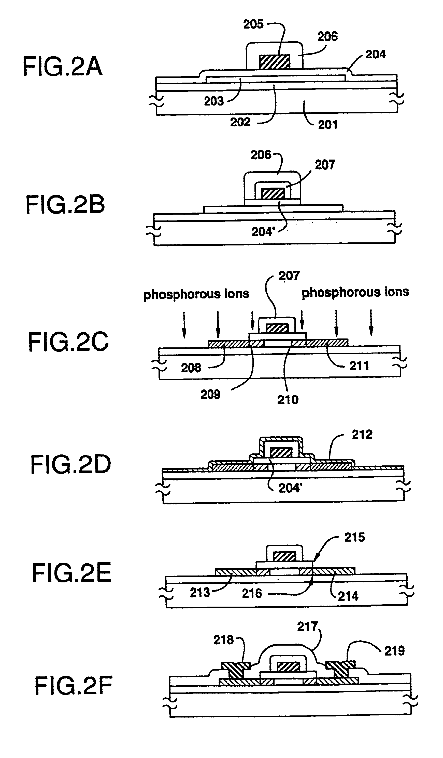
This example is an improvement of the Example 1, in which source and drain regions are provided with a silicide layer. Referring to FIG. 2A, the reference numeral 201 shows a Corning 7059 glass substrate, 202: a base film, 203: a silicon island, 204: an insulating film, 205: an Al gate electrode (200 nm-1 μm thick), and 206: a porous anodic oxide film (3000 Å-1 μm, e.g. 5000 Å thick). The same process as explained in the Example 1 is used to form these elements and the redundant explanation is omitted.

Referring to FIG. 2B, a barrier type anodic oxide film 207 of 1000-2500 Å thick is formed in the same manner as in the Example 1 after the formation of the porous anodic oxide 206. Then, a gate insulating film 204′ is formed by etching the insulating film 204 with the porous anodic oxide 206 used as a mask in a self-aligning manner.

Then, the porous anodic oxide 206 is removed by etching using the barrier type anodic oxide 207 as a mask. Further, ion doping of an impurity element (phosp...

example 3

This example is a further variation of Example 2, in which the order of the formation of a metal silicide and the ion doping is changed. Referring to FIG. 3A, on the Corning 7059 substrate 301 is formed a base oxide film 302, island-like crystalline semiconductor (e.g. silicon) region 303, silicon oxide film 304, aluminum gate electrode 305 of 2000 Å to 1 μm, and a porous anodic oxide film 306 of 6000 Å on the side of the gate electrode. These are formed in the same manner as in the Example 1 as discussed with reference to FIGS. 1A and 1B.

Further, a barrier type anodic oxide film 307 is formed to 1000-2500 Å in the same manner as in the Example 1. Subsequently, the silicon oxide film 304 is patterned into a gate insulating film 304′ in a self-aligning manner as shown in FIG. 3B.

Referring to FIG. 3C, the porous anodic oxide 306 is removed in order to expose a part of the gate insulating film 304′. Subsequently, a metal layer such as titanium film 308 is formed on the entire surface b...


PUM


Abstract

A TFT formed on an insulating substrate source, drain and channel regions, a gate insulating film formed on at least the channel region and a gate electrode formed on the gate insulating film. Between the channel region and the drain region, a region having a higher resistivity is provided in order to reduce an Ioff current. A method for forming this structure comprises the steps of anodizing the gate electrode to form a porous anodic oxide film on the side of the gate electrode; removing a portion of the gate insulating using the porous anodic oxide film as a mask so that the gate insulating film extends beyond the gate electrode but does not completely cover the source and drain regions. Thereafter, an ion doping of one conductivity element is performed. The high resistivity region is defined under the gate insulating film.

Description

BACKGROUND OF THE INVENTIONThe present invention relates to a semiconductor device and a manufacturing method thereof, in particular, the present invention is directed to an insulated gate field effect transistor of a thin film type formed on an insulating surface which may be a surface of an insulating substrate such as glass or an insulating film such as silicon oxide formed on a silicon wafer. Specifically, the present invention is applicable to a manufacture of a TFT (thin film transistor) formed on a glass substrate of which glass transition temperature (which is also called distortion point or distortion temperature) is 750° C. or lower.The semiconductor device manufactured in accordance with the present invention is applicable to a driving circuit for an active matrix device such as a liquid crystal display or an image sensor, or a three dimensional integrated circuit.TFTs have been well known to drive an active matrix type liquid crystal device or an image sensor. specifical...

Claims


Application Information

Patent Timeline
Patent Type & Authority Patents(United States)
IPC IPC(8): H01L29/786H01L21/02H01L29/45H01L29/66H01L27/12H01L21/321H01L21/336H01L29/40H01L21/311H01L21/316
CPCH01L27/127H01L21/31687H01L21/321H01L29/458H01L29/665H01L29/66598H01L29/66757H01L29/78621H01L29/78627H01L21/02145H01L21/02244H01L21/02258H01L27/124H01L21/31144H01L21/31116H01L21/31683
Inventor KONUMA, TOSHIMITSUSUGAWARA, AKIRAUEHARA, YUKIKOZHANG, HONGYONGSUZUKI, ATSUNORIOHNUMA, HIDETOYAMAGUCHI, NAOAKISUZAWA, HIDEOMIUOCHI, HIDEKITAKEMURA, YASUHIKO
Owner SEMICON ENERGY LAB CO LTD
Why Eureka
Try Eureka