Porous, film, wiring structure, and method of forming the same

a technology of porous film and wiring structure, which is applied in the direction of semiconductor devices, electrical equipment, semiconductor/solid-state device details, etc., can solve the problems of first conventional method having the problem of higher cost, delay in wiring time, and inability to implement a semiconductor integrated circuit with higher performance, so as to reduce the dielectric constant of the inter-layer dielectric, maintain sufficient mechanical strength and heat diffusing, and improve the effect of mechanical strength and heat conductivity

Inactive Publication Date: 2005-03-29
GK BRIDGE 1
View PDF5 Cites 15 Cited by
  • Summary
  • Abstract
  • Description
  • Claims
  • Application Information

AI Technical Summary

Benefits of technology

In the wiring structure according to the present invention, the porosity of the second inter-layer dielectric is higher than the porosity of the first inter-layer dielectric, so that the second inter-layer dielectric is lower in dielectric constant than the second inter-layer dielectric and higher in mechanical strength and heat conductivity than the first inter-layer dielectric. As a result, it is possible to reduce the dielectric constant of the inter-layer dielectric and retain the sufficient mechanical strength and heat diffusing property of the wiring structure.

Problems solved by technology

As the integration density of a semiconductor integrated circuit has increased, an increased wiring delay time resulting from an increase in wire-to-wire capacitance, which is a parasitic capacitance between metal wires, has presented an obstacle to the implementation of a semiconductor integrated circuit with higher performance.
However, the first conventional method has the problem of higher cost since it is necessary to prepare the solution of the siloxane polymer precursor.
Moreover, since the coated film is formed by coating the precursor solution on the substrate, the amount of silanol remaining, in the coated film is increased to cause such problems as a degassing phenomenon which is the elimination of moisture or the like in a thermal process step performed subsequently and the degradation of the porous film resulting from the absorption of moisture by the film.
On the other hand, the second conventional method has the problem of higher cost since it requires a special coating apparatus for controlling the speed at which the solvent eliminates from the wet gel.
Moreover, since a large number of silanol groups remain on the surfaces of the fine holes, they may cause serious degradation of the film because of high moisture absorption, unless they are removed.
It is therefore necessary to silylate the surfaces of silanol groups, resulting in a complicated process.
In the case of forming the wet gel by CVD, a special CVD apparatus different from a plasam CVD apparatus used normally in a semiconductor process is also required, which also increases cost.
Accordingly, it is difficult to adjust the dielectric constant of the porous film to 2 or less.

Method used


Image

  • Porous, film, wiring structure, and method of forming the same
  • Porous, film, wiring structure, and method of forming the same
  • Porous, film, wiring structure, and method of forming the same

Examples


embodiment 1

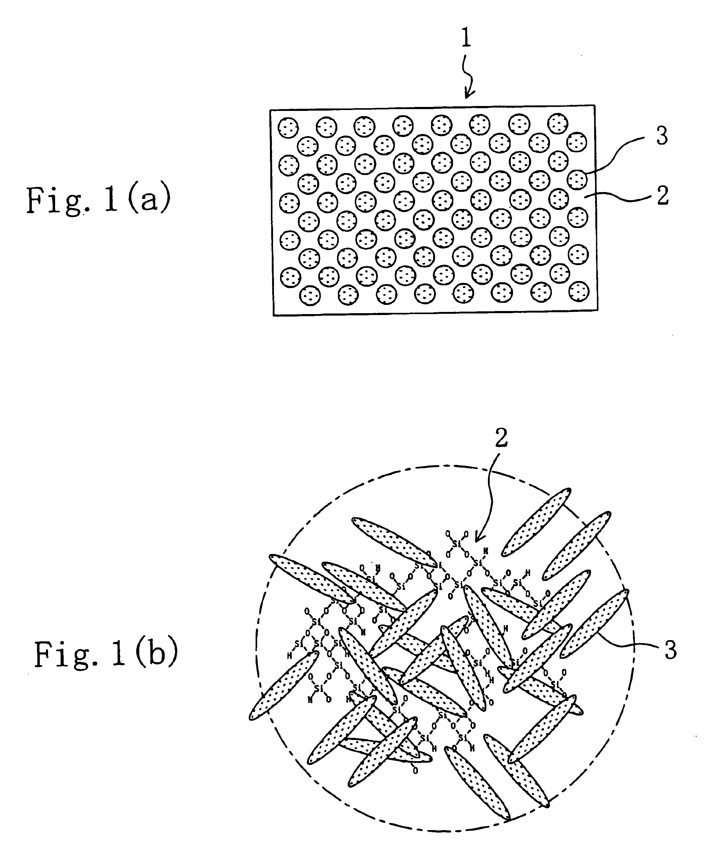
In accordance with a method of forming a porous film according to a first embodiment of the present invention, an organic-inorganic hybrid film is formed by plasma enhanced CVD using, as a reactive gas, a gas mixture of a silicon alkoxide gas and an organic compound gas and then a plasma process is performed with respect to the organic-inorganic hybrid film by using a plasma derived from a gas containing a reducing gas.

First, a gas mixture of a gas obtained by vaporizing vinyltrimethoxysilane (flowrate: 1 ml / min) as the siliconalkoxide and an acetylene gas (flow rate: 100 sccm) as the organic compound gas is introduced under pressure of 1.0 Torr into a vacuum chamber. On the other hand, RF power of 13.56 MHz is applied with electric power of 500 W between counter electrodes to generate a plasma derived from the gas mixture, whereby the organic-inorganic hybrid film having a siloxane skeleton and a thickness of 320 nm is deposited on a substrate. The plasma enhanced CVD process was p...

embodiment 2

In accordance with a method of forming a porous film according to a second embodiment of the present invention, an organic-inorganic hybrid film is formed by plasma enhanced CVD, using, as a reactive gas, a gas mixture of a silicon alkoxide gas and an organic compound gas and then a thermal process is performed with respect to the organic-inorganic hybrid film in an atmosphere containing a reducing gas.

First, the organic-inorganic hybrid film is formed by plasma enhanced CVD using, as the reactive gas, a gas mixture of a gas obtained by vaporizing vinyltrimethoxysilane as the silicon alkoxide and an acetylene gas as the organic compound gas, similarly to the first embodiment.

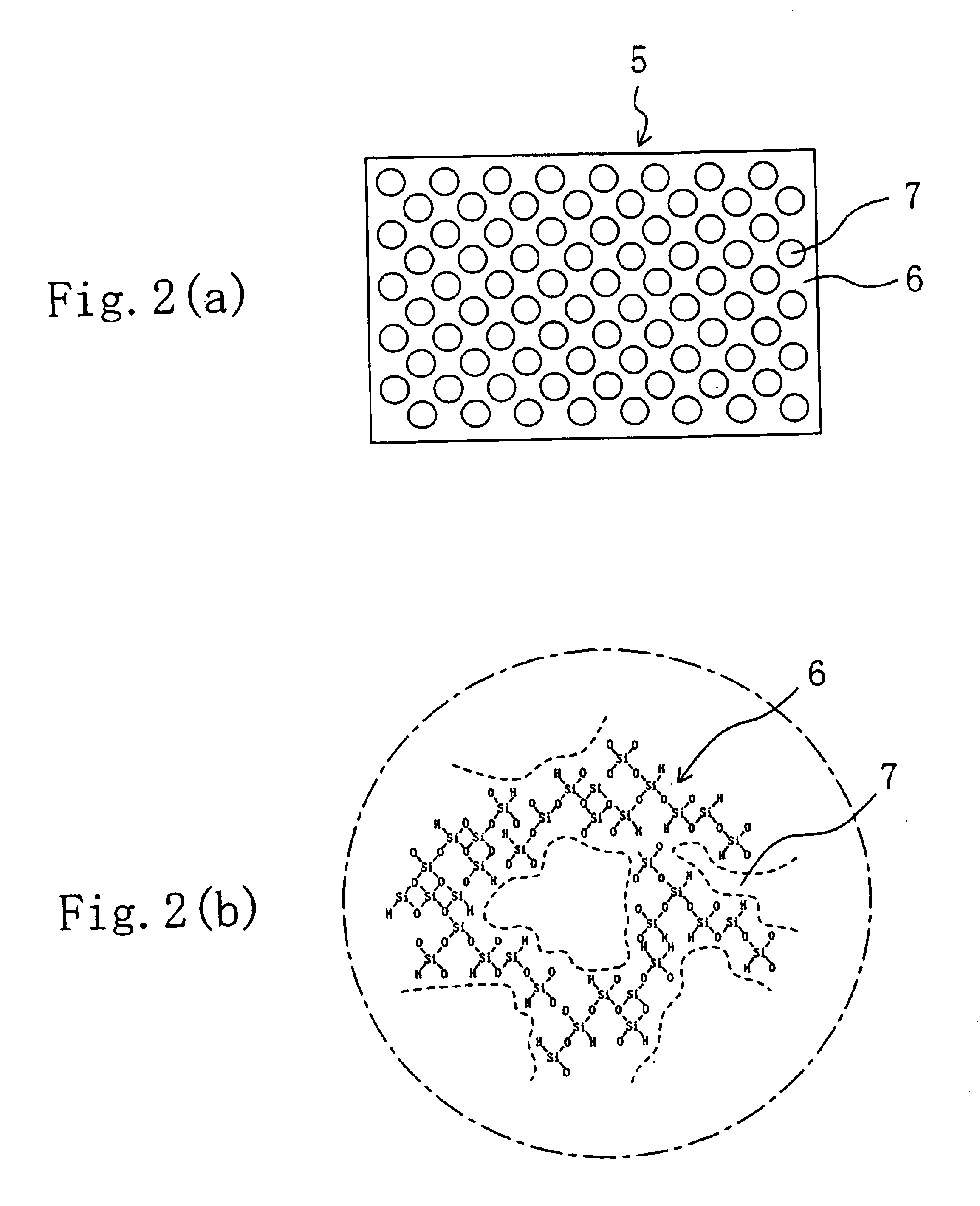
Next, a thermal process at a temperature of about 400° C. is performed with respect to the organic-inorganic hybrid film by using, e.g., an electric furnace in an atmosphere containing a reducing gas which is composed of a gas mixture of a hydrogen gas, a nitrogen gas, and an oxygen gas.

According to the second e...

embodiment 3

In accordance with a method of forming a porous film according to a third embodiment of the present invention, an organic-inorganic hybrid film is formed by plasma enhanced CVD using, as a reactive gas, a gas mixture of a silicon alkoxide gas and an organic compound gas and then a plasma process is performed with respect to the organic-inorganic hybrid film using a plasma derived from an ammonia gas and an oxygen gas.

First, the organic-inorganic hybrid film is formed by plasma enhanced CVD using, as the reactive gas, a gas mixture of a gas obtained by vaporizing vinyltrimethoxysilane as the silicon alkoxide and an acetylene gas as the organic compound gas, similarly to the first embodiment.

Next, a gas mixture of an ammonia gas (flow rate: 100 sccm), an argon gas (flow rate: 1000 sccm) as a dilute gas, and an oxygen gas (flow rate: 100 sccm) is introduced under pressure of 5 Torr into a vacuum chamber and RF power of 13.56 MHz is applied with electric power of 500 W between counter e...


PUM


Abstract

An organic-inorganic hybrid film is deposited on a substrate by introducing, into a vacuum chamber, a gas mixture of a silicon alkoxide and an organic compound and generating a plasma derived from the gas mixture. Then, a hydrogen plasma process is performed with respect to the organic-inorganic hybrid film by introducing, into the vacuum chamber, a gas containing a reducing gas and generating a plasma derived from the gas. As a result, an organic component in the organic-inorganic hybrid film eliminates therefrom and numerous fine holes are formed in hollow portions from which the organic component has eliminated, whereby a porous film composed of the organic-inorganic hybrid film is obtained.

Description

BACKGROUND OF THE INVENTIONThe present invention relates to a method of forming a porous film used as, e.g., an inter-layer dielectric in a semiconductor integrated circuit device.As the integration density of a semiconductor integrated circuit has increased, an increased wiring delay time resulting from an increase in wire-to-wire capacitance, which is a parasitic capacitance between metal wires, has presented an obstacle to the implementation of a semiconductor integrated circuit with higher performance. The wiring delay time is a so-called RC delay which is proportional to the product of the resistance of the metal wire and the wire-to-wire capacitance.To reduce the wiring delay time, therefore, it is necessary to reduce the resistance of the metal wire or the wire-to-wire capacitance.As a method of reducing the wire-to-wire capacitance, the reduction of the dielectric constant of an inter-layer dielectric formed between the metal wires has been considered. As an inter-layer diel...

Claims


Application Information

Patent Timeline
Patent Type & Authority Patents(United States)
IPC IPC(8): H01L21/70H01L23/52H01L23/522H01L21/02H01L23/532H01L21/768H01L21/316H01L21/312
CPCH01L21/02126H01L21/022H01L21/02203H01L21/02216H01L21/02274H01L21/02282H01L21/02337H01L21/0234H01L21/3122H01L21/31695H01L21/76802H01L21/76807H01L21/76814H01L21/7682H01L21/76826H01L21/76835H01L23/5222H01L23/5329H01L2924/0002H01L2221/1047H01L2924/12044H01L2924/00H01L2221/1036
Inventor AOI, NOBUO
Owner GK BRIDGE 1
Why Eureka
Try Eureka