Patterning solution deposited thin films with self-assembled monolayers

a technology of self-assembled monolayers and thin films, which is applied in the direction of liquid/solution decomposition chemical coating, conductive pattern formation, resistor manufacturing, etc., can solve the problems of degrading the desirable material properties (e.g., electrical, optical, magnetic or structural properties) of the thin film, and both complex and costly, and degrading the deposited thin film

Inactive Publication Date: 2005-05-03
IBM CORP
View PDF7 Cites 112 Cited by
  • Summary
  • Abstract
  • Description
  • Claims
  • Application Information

AI Technical Summary

Benefits of technology

[0032]It is an object of the present invention to provide a low-cost method of forming a patterned ...

Problems solved by technology

Etching spin- or dip-coated thin films exposes the deposited material to potentially harsh etching solutions or environments and may degrade the desirable materials properties (e.g., electrical, optical, magnetic, or structural) of the thin film.
Etching also requires multiple processing steps making it both more complex and costly.
Interaction between the thin film material and the resist, radiation, or solvents/developer used in the lithography process may also degrade the deposited thin film.
These focused beam techniques are serial “writing” processes that are slow and therefore inherently more costly when large areas of the film must be modified.
These applications of focused beams to pattern thin films can lead to redeposition of undesirable materials, in the case of pyrolysis, and to possible material degradation by solvents used to remove the remaining metallo-organics, in the case of local decomposition.
In general, lithographic and focused beam techniques all require the use of a relatively complicated and costly apparatus to prepare patterned thin films.
Resists, solvents, and developer used in these processes are also consumed, thus producing undesira...

Method used


Image

  • Patterning solution deposited thin films with self-assembled monolayers
  • Patterning solution deposited thin films with self-assembled monolayers
  • Patterning solution deposited thin films with self-assembled monolayers

Examples


example 1

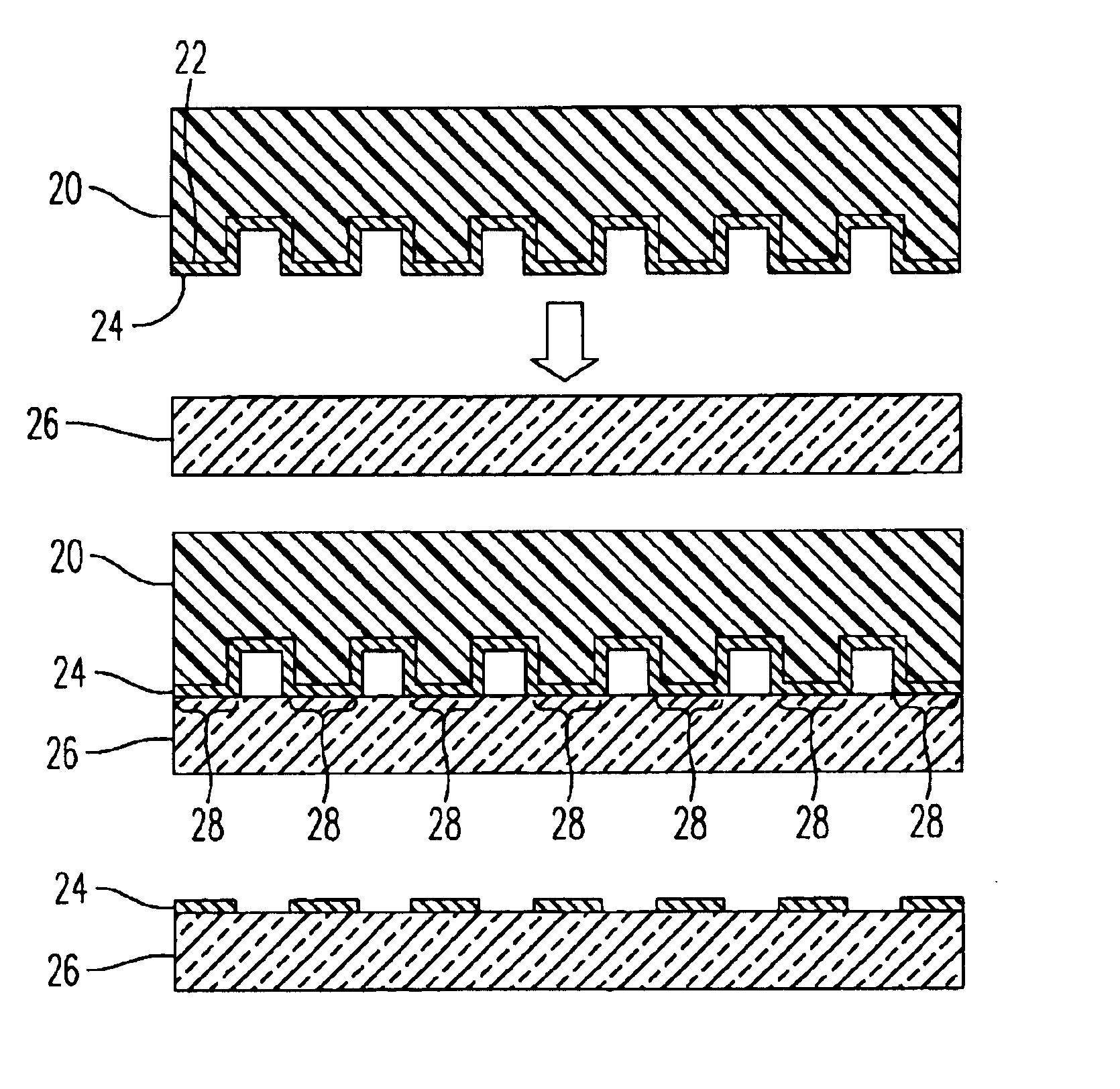
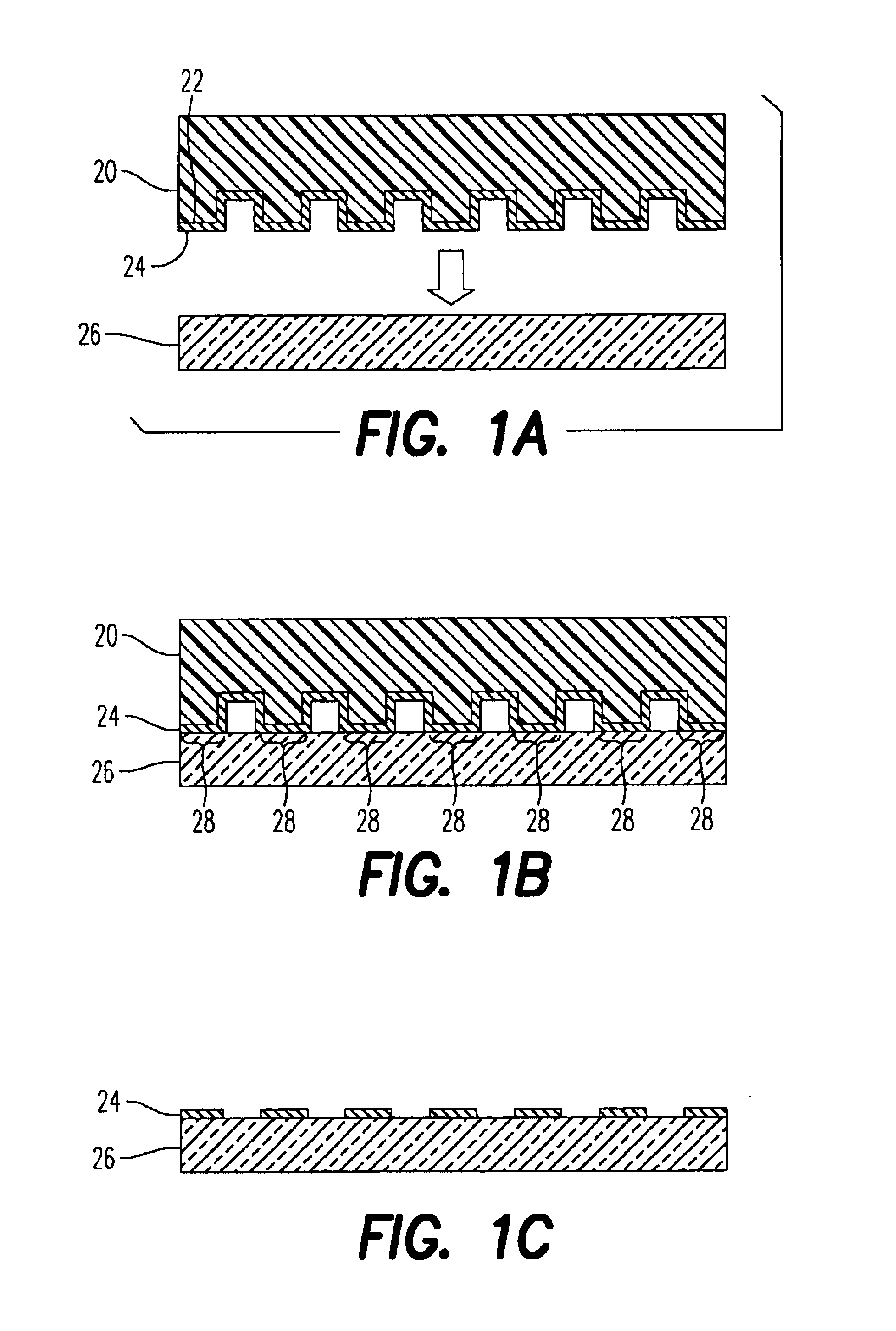
[0099]A template having an exposed and developed photoresist pattern was fabricated by photolithography. A 10:1 (w:w or v:v) mixture of PDMS-Sylgard Silicone Elastomer 184 and Sylgard Curing Agent 184 (Dow Corning Corp., Midland, Mich.) was degassed under vacuum for about 10 minutes, then the mixture was poured over the template. The PDMS cured at 65° C. within 60 minutes to produce an elastomeric stamp. After cooling to room temperature, the PDMS stamp was carefully peeled from the template. A thermally grown silicon dioxide surface on an n-type silicon wafer was patterned with a self-assembled molecular monolayer of octadecyl phosphonic acid by the elastomeric stamp using microcontact printing, as illustrated in FIGS. 1A-C.

[0100]The phosphonic acid terminal head group acts to bind to the hydrophillic silicon dioxide surface and the long octadecyl chain imparts a contrasting hydrophobic surface. Patterning the silicon dioxide surface with octadecylphosphonic acid provides a substra...

example 2

[0103]A silicon dioxide surface on an n-type silicon wafer was patterned by microcontact printing with a self-assembled monolayer of the fluorinated silane having the formula (tridecafluoro 1,1,2,2-tetrahydrooctyl)trichlorosilane. The trichlorosilane head group acts to bind to the hydrophilic silicon dioxide surface and the fluorinated hydrocarbon tail group imparts a contrasting hydrophobic surface, akin to Teflon. The chemical differentiation across the substrate surface was similarly used to define the pattern of deposited thin films of various organic-inorganic hybrid materials.

[0104]Each of the following organic-inorganic hybrid materials were used:[0105](1) phenethylammonium tin iodide having the formula (C6H5C2H4NH3)2SnI4 from a solution in methanol;[0106](2) butylammonium methylammonium tin iodide having the formula (C4H9NH3)2CH3NH3Sn2I7 from a solution in N,N-dimethylformamide;[0107](3) phenethylammonium methylammonium tin iodide having the formula (C6H5C2H4NH3)2CH3NH3Sn2I7...

example 3

[0112]As silicon dioxide surface on an n-type silicon wafer is patterned by microcontact printing with a self-assembled monolayer of (tridecafluoro 1,1,2,2-tetrahydrooctyl)trichlorosilane (a fluorinated silane).

[0113]The chemical differentiation on the substrate surface is used to define the pattern of deposited thin film of the copolymer polymethyl methacrylate / methyl methacrylate (PMMA / MMA) from a solution in ethyl lactate. PMMA / MMA is used as an insulator in electrical applications and as a material to prepare microlenses for optical applications. It is also a resist for e-beam lithography.

[0114]The method of the present invention can be used to define large features in resist and e-beam lithography can be used to pattern small features. The hybrid technique resulting from the combination of these methods allows patterning of both large and small features on the substrate thereby reducing the time and the overall cost of patterning relative to using e-beam lithography alone.


PUM

PropertyMeasurementUnit
Flexibilityaaaaaaaaaa
Semiconductor propertiesaaaaaaaaaa

Abstract

The present invention provides a method of forming a patterned thin film on a surface of a substrate having thereon a patterned underlayer of a self-assembled monolayer. The method comprises depositing a thin film material on the self-assembled monolayer to produce a patterned thin film on the surface of the substrate. The present invention further provides processes for preparing the self-assembled monolayer. The present invention still further provides solution-based deposition processes, such as spin-coating and immersion-coating, to deposit a thin film material on the self-assembled monolayer to produce a patterned thin film on the surface of the substrate.

Description

BACKGROUND OF THE INVENTION[0001]1. Field of the Invention[0002]The present invention relates generally to the patterning of a thin film on a surface. More particularly, the present invention relates to a method of depositing by a solution-based technique a patterned thin film onto a surface that has been selectively patterened with a self-assembled molecular monolayer.[0003]2. Description of the Prior Art[0004]Solution-based thin film deposition processes, such as spin-coating and immersion-coating, i.e., dip-coating, provide simple, low-cost, low-temperature routes to thin film deposition on large-area solid substrates.[0005]Spin-coating and dip-coating are long-tested techniques commonly used to deposit thin films of a wide variety of materials for a broad range of applications. These materials include, as examples, organic materials, such as small molecules, oligomers, polymers, and photoresists; organic-inorganic hybrid materials; soluble inorganic materials, such as salts; sus...

Claims


Application Information

Patent Timeline
IPC IPC(8): B05D5/12B44C1/165B44C1/16C03C25/68C03C15/00H01L21/02H01L21/30G03F7/00G03F7/16G03F7/40H01L51/00H01L51/40H05K3/12
CPCB82Y10/00B82Y30/00G03F7/0002G03F7/165Y10S428/914G03F7/40H01L51/0017H05K3/12H10K71/231
Inventor KAGAN, CHERIE R.BREEN, TRICIA LYNNKOSBAR, LAURA LOUISE
Owner IBM CORP
Why Eureka
Try Eureka