Semiconductor device, manufacturing method thereof, and display device

a technology of semiconductor devices and semiconductors, applied in the direction of transistors, optics, instruments, etc., can solve the problems of large requirements, difficult reduction of off current values, and inability to meet the requirements of a large number of requirements, so as to prevent the possibility of a tft threshold voltage variation

Inactive Publication Date: 2005-05-24
SEMICON ENERGY LAB CO LTD
View PDF18 Cites 52 Cited by
  • Summary
  • Abstract
  • Description
  • Claims
  • Application Information

AI Technical Summary

Benefits of technology

[0063]After the first crystalline semiconductor film is formed, the second amorphous semiconductor film is formed and crystallized by irradiation of laser light. Thus, the first crystalline semiconductor film functions to relax an internal stress at laser irradiation from a different kind of film, the base insulating film and the light shielding film. In addition, the first c

Problems solved by technology

There is a problem that compatibility of an increase in an aperture ratio and a reduction in a photo leak current or compatibility of an increase in the aperture ratio and a reduction in an off current value is difficult in the above-mentioned conventional pixel structure or TFT structure.
Such a requirement becomes a large problem in the case where a pitch of respe

Method used


Image

  • Semiconductor device, manufacturing method thereof, and display device
  • Semiconductor device, manufacturing method thereof, and display device
  • Semiconductor device, manufacturing method thereof, and display device

Examples


embodiment mode 1

(Embodiment Mode 1)

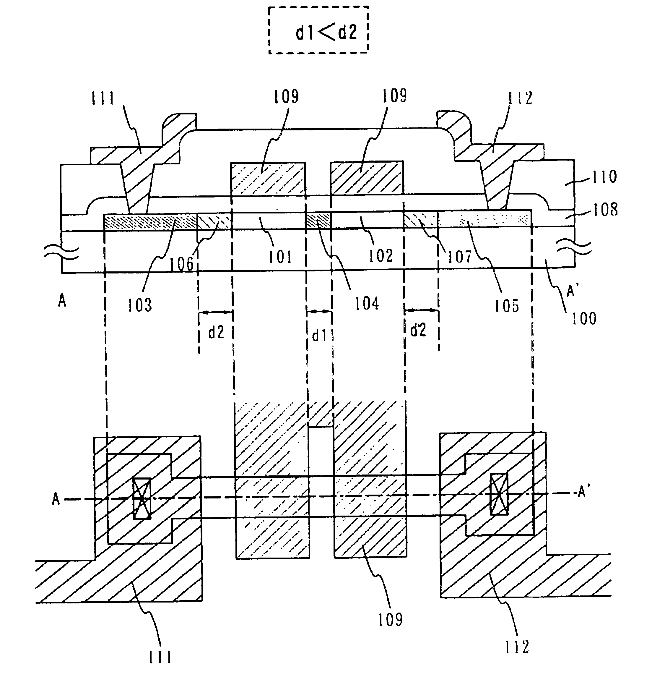
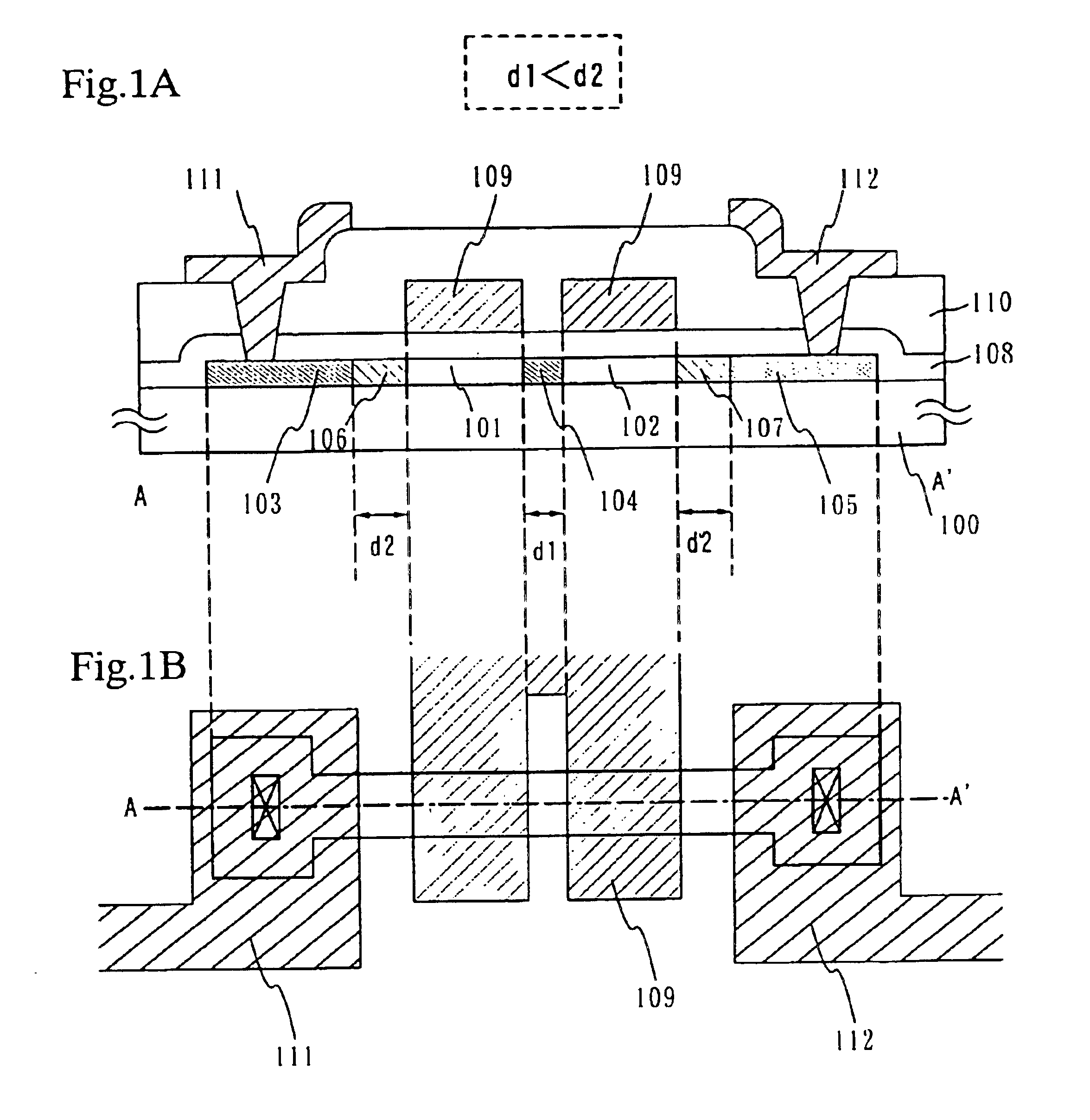
[0092]One example in the case of applying the present invention to a TFT with a double gate structure is shown in FIGS. 1A and 1B and described below.

[0093]In FIGS. 1A and 1B, reference numeral 100 denotes a substrate, 101 and 102 denote channel forming regions, 103 and 105 denote a source region and a drain region, 104 denotes a high concentration impurity region, 106 and 107 denote low concentration impurity regions (LDD regions), 108 denotes a gate insulating film, 109 denotes gate electrodes, 110 denotes an interlayer insulating film, and 111 and 112 denote a source electrode and a drain electrode. Note that FIG. 1A is a cross sectional view taken along the dotted line A-A′ of FIG. 1B which is a top view of a TFT.

[0094]The present invention is characterized in that only the high concentration impurity region 104 is formed as a region sandwiched by the two channel forming regions 101 and 102. An interval d1 between the adjacent gate electrodes 109, that is, a w...

embodiment mode 2

(Embodiment Mode 2)

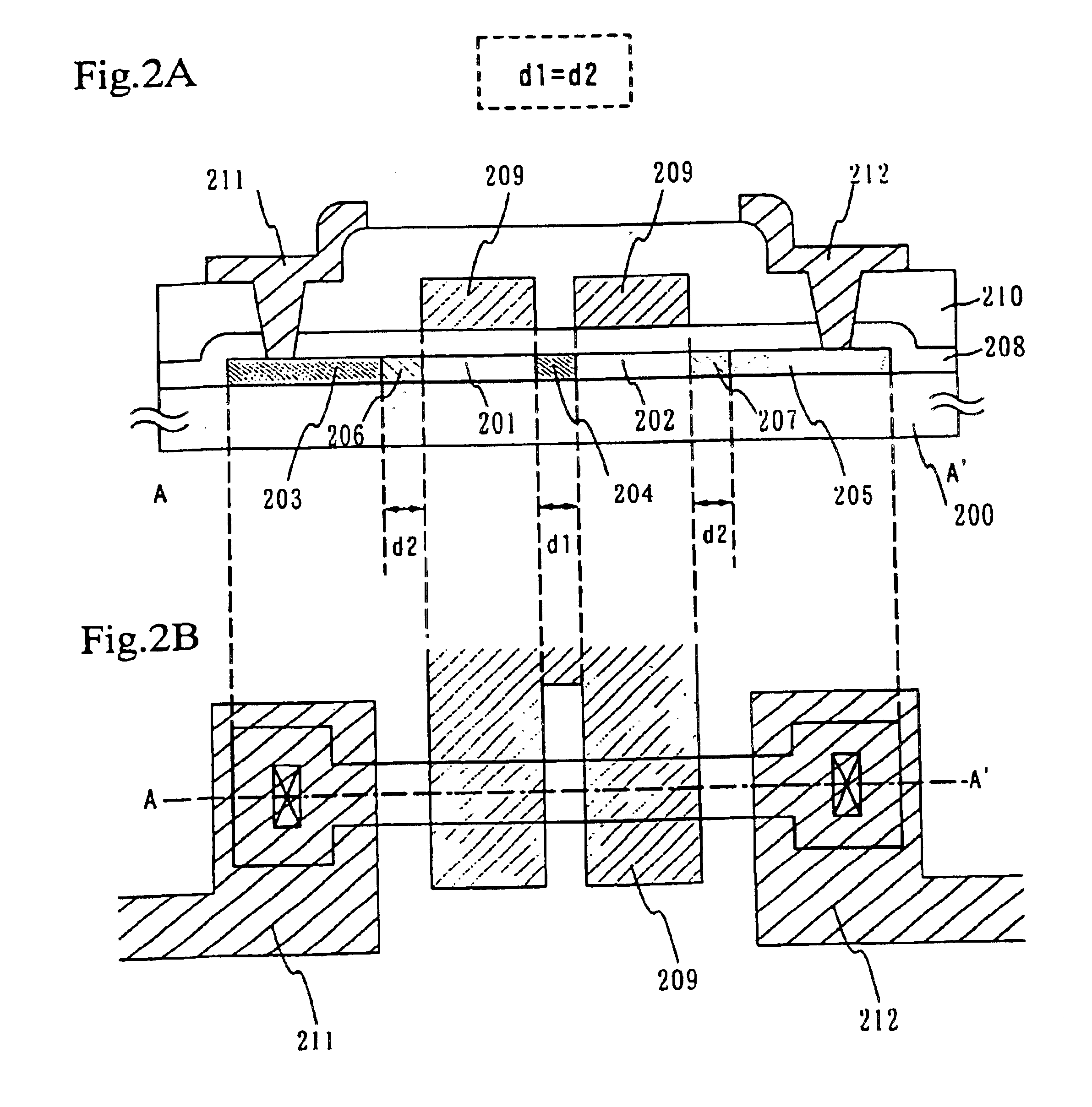
[0108]Although the example in which d12 is set is indicated in Embodiment Mode 1, one example in the case where Embodiment Mode 2 of the present invention in which d1=d2 is set is applied to a TFT with a double gate structure is shown in FIGS. 2A and 2B and described below.

[0109]In FIGS. 2A and 2B, reference numeral 200 denotes a substrate, 201 and 202 denote channel forming regions, 203 and 205 denote a source region and a drain region, 204 denotes a high concentration impurity region, 206 and 207 denote low concentration impurity regions (LDD regions), 208 denotes a gate insulating film, 209 denotes gate electrodes, 210 denotes an interlayer insulating film, and 211 and 212 denote a source electrode and a drain electrode. Note that FIG. 2A is a cross sectional view taken along a dotted line A-A′ of FIG. 2B which is a top view of a TFT.

[0110]The present invention is characterized in that only the high concentration impurity region 204 is formed as a region sandwi...

embodiment mode 3

(Embodiment Mode 3)

[0111]This embodiment mode is indicated in FIG. 21. A first light shielding layer 1102 is formed to correspond to a channel forming region of a semiconductor layer 1105 on a substrate 1101. The first light shielding layer 1102 is formed of a non-translucent material with a heat resistance such as W, Ta, Ti, or silicide thereof. The non-translucent material is selected to keep stability with respect to a thermal treatment step at 500° C. or higher which is performed for the semiconductor layer and the like as a later step. A first insulating layer is formed from a silicon oxynitride film 1103 and a silicon oxide film 1104. The surface of the silicon oxide film may be leveled by chemical mechanical polishing (CMP).

[0112]The semiconductor layer 1105 is formed from a polycrystalline semiconductor layer obtained by crystallizing an amorphous semiconductor film using thermal treatment and have a thickness of about 30 nm to 750 nm. A second insulating film 1106 is formed...


PUM


Abstract

A multi-gate structure is used and a width (d1) of a high concentration impurity region sandwiched by two channel forming regions in a channel length direction is set to be shorter than a width (d2) of low concentration impurity regions in the channel length direction. Thus, a resistance of the entire semiconductor layer of a TFT which is in an on state is reduced to increase an on current. In addition, a carrier life time due to photoexcitation produced in the high concentration impurity region can be shortened to reduce light sensitivity.

Description

BACKGROUND OF THE INVENTION[0001]1. Field of the Invention[0002]The present invention relates to a semiconductor device which has a circuit composed of a thin film transistor (hereinafter referred to as a TFT) and a manufacturing method thereof. The present invention relates to, for example, an electro-optical device represented by a liquid crystal display panel and electronic equipment in which such an electro-optical device is mounted as a part.[0003]Note that in this specification, a semiconductor device indicates a general device which functions by utilizing semiconductor characteristics, and an electro-optical device, a semiconductor circuit, and an electronic device are each a semiconductor device.[0004]2. Description of the Related Art[0005]In recent years, the development of a semiconductor device, which has a large area integrated circuit manufactured from a thin film transistor (TFT) using a semiconductor thin film (about several nm to several hundred nm in thickness) form...

Claims


Application Information

Patent Timeline
IPC IPC(8): G02F1/13G02F1/1362H01L21/02H01L21/336H01L21/70H01L29/66H01L29/786H01L21/84H01L27/12H01L21/77H01L27/13
CPCG02F1/136209G02F1/136286H01L27/1255H01L29/78621H01L29/78633H01L29/78645H01L29/78675H01L29/78696H01L29/66757G02F1/13454G02F1/136213G02F1/136227G02F2202/105H01L27/1222
Inventor SHIBATA, HIROSHIMAEKAWA, SHINJI
Owner SEMICON ENERGY LAB CO LTD
Why Eureka
Try Eureka