Method of manufacturing a semiconductor device with a vertical drain drift layer of the alternating-conductivity-type

a technology of alternating conductivity and semiconductor devices, which is applied in the direction of semiconductor devices, basic electric elements, electrical equipment, etc., can solve the problems of increasing on-loss, difficult for the presently available selective etching techniques, and difficult for the presently available epitaxial growth techniques to grow a high-quality single crystal layer in such a narrow and deep trench. , to achieve the effect of high breakdown voltage, convenient narrowing and high current density

Inactive Publication Date: 2005-05-31
FUJI ELECTRIC CO LTD
View PDF28 Cites 25 Cited by
  • Summary
  • Abstract
  • Description
  • Claims
  • Application Information

AI Technical Summary

Benefits of technology

[0012]Since the vertical first regions or the vertical second regions are built in by connecting buried diffusion unit regions vertically, the impurity concentration in the vertical first regions or the vertical second regions exhibits almost isotropic distributions around the scattered diffusion centers aligned vertically. Although the impurity concentration distribution in the vertical first regions or the vertical second regions is not uniform, pn-junction planes between the vertical first regions and the vertical second regions are almost flat. Since the narrow vertical first regions, which provide a vertical current path in the ON-state of the semiconductor device, can be doped heavily, the alternating conductivity type layer according to the invention facilitates realizing a high current density. Since the vertical second regions are depleted in the OFF-state of the semiconductor device by the depletion layers expanding laterally from the pn-junctions on both sides thereof, alternating conductivity type layer according to the invention facilitates realizing also a high breakdown voltage.
[0013]The vertical first regions and the vertical second regions having the structures as described above are formed according to the invention by repeating the step of laminating epitaxi...

Problems solved by technology

Although a high breakdown voltage is obtained by thickening n-type drain drift layer 12, thick n-type drain drift layer 12 inevitably causes on-resistance increase, that further causes on-loss increase.
It is difficult for the presently available selective etching techniques to dig the trenches with such a large aspect...

Method used


Image

  • Method of manufacturing a semiconductor device with a vertical drain drift layer of the alternating-conductivity-type
  • Method of manufacturing a semiconductor device with a vertical drain drift layer of the alternating-conductivity-type
  • Method of manufacturing a semiconductor device with a vertical drain drift layer of the alternating-conductivity-type

Examples


first embodiment

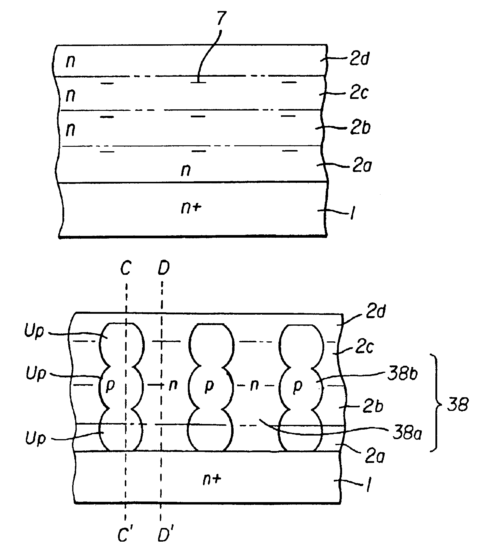
[0040]FIG. 1 is a cross sectional view of a vertical n-channel MOSFET according to a first embodiment of the invention.

[0041]Referring now to FIG. 1, the vertical n-channel MOSFET includes an n+-type drain layer 11 with low electrical resistance; a drain electrode 18 in electrical contact with the back surface of n+-type drain layer 11; an alternating-conductivity-type drain drift layer 38 on n+-type drain layer 11; p-type base regions (p-type well regions or channel diffusion regions) 13 formed selectively in the surface portion of drain drift layer 38; a heavily doped n+-type source region 14 formed selectively in the surface portion of p-type base region 13; a heavily doped p+-type contact region 19 formed selectively in the surface portion of p-type base region 13; a gate insulation film 15 on the extended portion of p-type base region 13 extended between n+-type source region 14 and an n-type drain region 21 described layer; a polysilicon gate electrode 16 on gate insulation fi...

second embodiment

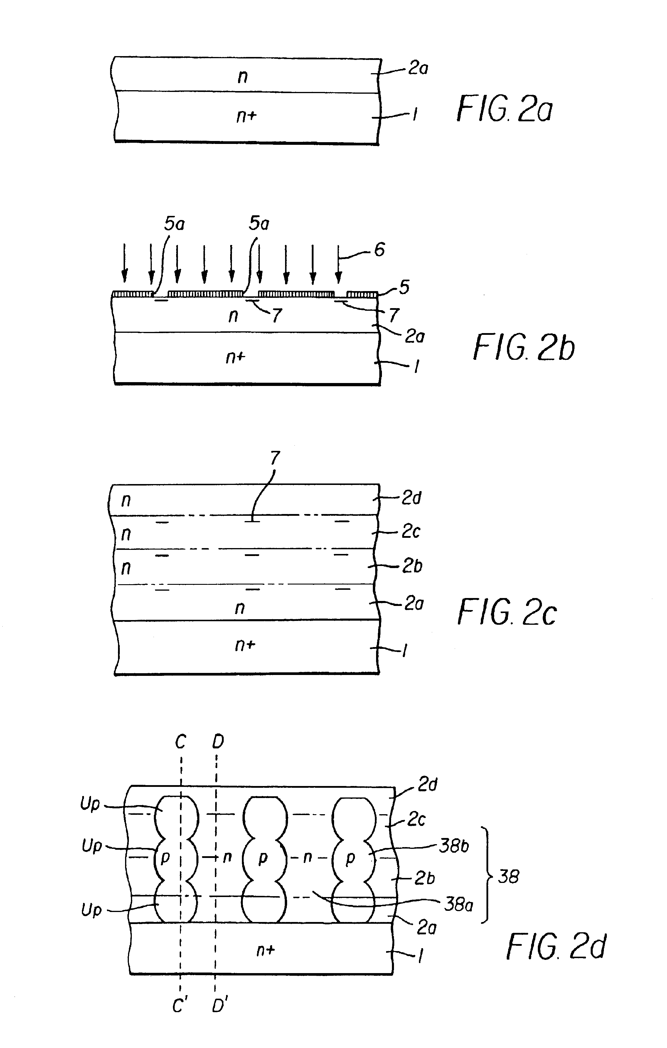
[0061]FIGS. 4(a) through 4(e) are cross sectional views for explaining a method of manufacturing a vertical MOSFET according to a second embodiment of the invention.

[0062]The vertical MOSFET according to the second embodiment includes a drain drift layer 48, that is different, as shown in FIG. 4(e), from drain drift layer 38 of the vertical MOSFET according to the first embodiment. Referring now to FIG. 4(e), drain drift layer 48 includes n-type drift current path regions 48a, each formed of n-type buried diffusion unit regions Un connected vertically with each other across p-type epitaxially grown layers 42a through 42d laminated with each other.

[0063]Referring now to FIG. 4(a), a p-type epitaxially grown layer 42a is laminated on an n-type semiconductor substrate 1 with low electrical resistance.

[0064]Referring now to FIG.4(b), a resist mask 5, having narrow windows 5a for ion implantation opened at a certain interval, is formed on p-type epitaxially grown layer 42a by photolithog...

third embodiment

[0070]FIGS. 5(a) through 5(f) are cross sectional views for explaining a method of manufacturing a vertical MOSFET according to a third embodiment of the invention.

[0071]The vertical MOSFET according to the third embodiment has the same structure with that of the vertical MOSFET according to the first embodiment shown in FIG. 1. In forming the alternating conductivity type layer of the vertical MOSFET according to the first embodiment, n-type epitaxially grown layers 2a through 2d are laminated. In forming the alternating conductivity type layer of the vertical MOSFET according to the third embodiment, a step of laminating an n-type layer and a steps of implanting n-type impurities into the entire surface portion of the as laminated n-type layer are repeated.

[0072]Referring now to FIG. 5(a), a first n-type layer 2a′ is epitaxially grown on an n-type semiconductor substrate with low electrical resistance.

[0073]Referring now to FIG. 5(b), n-type impurity phosphorus ions 3 are implante...


PUM


Abstract

A semiconductor device includes an improved drain drift layer structure of alternating conductivity types, that is easy to manufacture, and that facilitates realizing a high current capacity and a high breakdown voltage and to provide a method of manufacturing the semiconductor device. The vertical MOSFET according to the invention includes an alternating-conductivity-type drain drift layer on an n+-type drain layer as a substrate. The alternating-conductivity-type drain drift layer is formed of n-type drift current path regions and p-type partition regions alternately arranged laterally with each other. The n-type drift current path regions and p-type partition regions extend in perpendicular to n+-type drain layer. Each p-type partition region is formed by vertically connecting p-type buried diffusion unit regions Up. The n-type drift current path regions are residual regions, left after connecting p-type buried diffusion unit regions Up, with the conductivity type thereof unchanged. The alternating-conductivity-type drain drift layer is formed by repeating the step of epitaxial layer growth and the step of implanting p-type impurity ions and by diffusing the impurity ions at once from the impurity sources located on multiple levels.

Description

[0001]This is a Division of application Ser. No. 09 / 693,574 filed Oct. 20, 2000 now U.S. Pat. No. 6,611,021.FIELD OF THE INVENTION[0002]The present invention relates to a semiconductor structure applicable to semiconductor devices, such as a MOSFET (an insulated gate field effect transistor), an IGBT (an insulated gate bipolar transistor), a bipolar transistor and a diode, which simultaneously exhibit a high breakdown voltage and a high current capacity. More specifically, the present invention relates to a semiconductor device structure including a vertical drain drift layer and the method of manufacturing the semiconductor device.BACKGROUND ART[0003]The semiconductor devices may be roughly classified into a lateral device, that arranges the main electrodes thereof on one major surface, and a vertical device that distributes the main electrodes thereof on two major surfaces facing opposite to each other. In the vertical device, a drift current flows in the ON-state of the device an...

Claims


Application Information

Patent Timeline
IPC IPC(8): H01L21/02H01L21/336H01L29/78H01L29/66H01L29/08H01L29/10H01L29/02H01L29/06
CPCH01L29/0634H01L29/7802H01L29/66712H01L29/0847H01L29/1095
Inventor ONISHI, YASUHIKOFUJIHIRA, TATSUHIKOIWAMOTO, SUSUMUSATO, TAKAHIRO
Owner FUJI ELECTRIC CO LTD
Why Eureka
Try Eureka