Electron beam apparatus and device manufacturing method using same

a technology of electron beam and manufacturing method, which is applied in the direction of semiconductor/solid-state device testing/measurement, instruments, heat measurement, etc., can solve the problems of primary electron beams having energy over the aforementioned range that are not suitable for inspection, and the distortion and aberration cannot be sufficiently reduced, so as to reduce aberration and distortion, increase the conductivity effect, and improve the effect of potential uniformity

Inactive Publication Date: 2005-06-21
EBARA CORP
View PDF8 Cites 79 Cited by
  • Summary
  • Abstract
  • Description
  • Claims
  • Application Information

AI Technical Summary

Benefits of technology

[0006]To achieve the above object, in one embodiment of the present invention, a mapping type defect detecting apparatus includes an electron source for irradiating a primary electron beam to the surface of a sample such as a wafer, an electro-optical mapping system for enlarging the image of the secondary electrons emitted from the surface of the sample to focus the enlarged secondary electrons on a detector, and an image processing system for processing a signal from the detector, wherein the electron beam incident on the sample is optimized to have beam energy in a range of 2 to 4 keV, thereby reducing a secondary electron emission efficiency from the sample to less than one. This causes the sample to be negatively charged to significantly reduce image distortions. Since reasonable conductivity occurs on the surface of the sample in this energy region when the sample is a mixture of a metal and an insulating material, no extreme potential difference will be produced by the charging between the metal and insulating material. It is therefore possible to form an image with less distortion and aberration when the secondary electrons emitted from the surface of the sample is focused on the detector through the optical mapping system.
[0007]It should be noted that the conductivity effect is insufficient with incident beam energy smaller than the range mentioned above, resulting in a failure in a sufficient reduction in distortion and aberration. On the other hand, the primary electron beam having the energy exceeding the aforementioned range is not suitable for inspection because devices could be damaged by an excessive Joule heat effect and damaging effect. Since it takes a few minutes for a conductivity effect to appear on the surface of a wafer, which will prevent a high-throughput process, a surface potential may be previously uniformed by such means as laser irradiation and secondary electron source, thereby achieving high throughput.
[0010]In addition, the sample may be irradiated simultaneously with a laser or an electron beam to increase the conductivity effect on the surface of the sample, to make the potential more uniform on the surface of the sample, as compared with the irradiation of the electron beam alone, and to detect an electron beam with less aberration and distortion.
[0013]The primary electron beam having beam energy in a range of 2 to 4 keV can negatively charge an insulating material on the surface of the sample to reduce overcharging. The optical mapping system has a resolution equal to or less than 0.1 μm, and a maximum image height equal to or larger than 50 μm in the field of view.

Problems solved by technology

It should be noted that the conductivity effect is insufficient with incident beam energy smaller than the range mentioned above, resulting in a failure in a sufficient reduction in distortion and aberration.
On the other hand, the primary electron beam having the energy exceeding the aforementioned range is not suitable for inspection because devices could be damaged by an excessive Joule heat effect and damaging effect.

Method used


Image

  • Electron beam apparatus and device manufacturing method using same
  • Electron beam apparatus and device manufacturing method using same
  • Electron beam apparatus and device manufacturing method using same

Examples


first embodiment

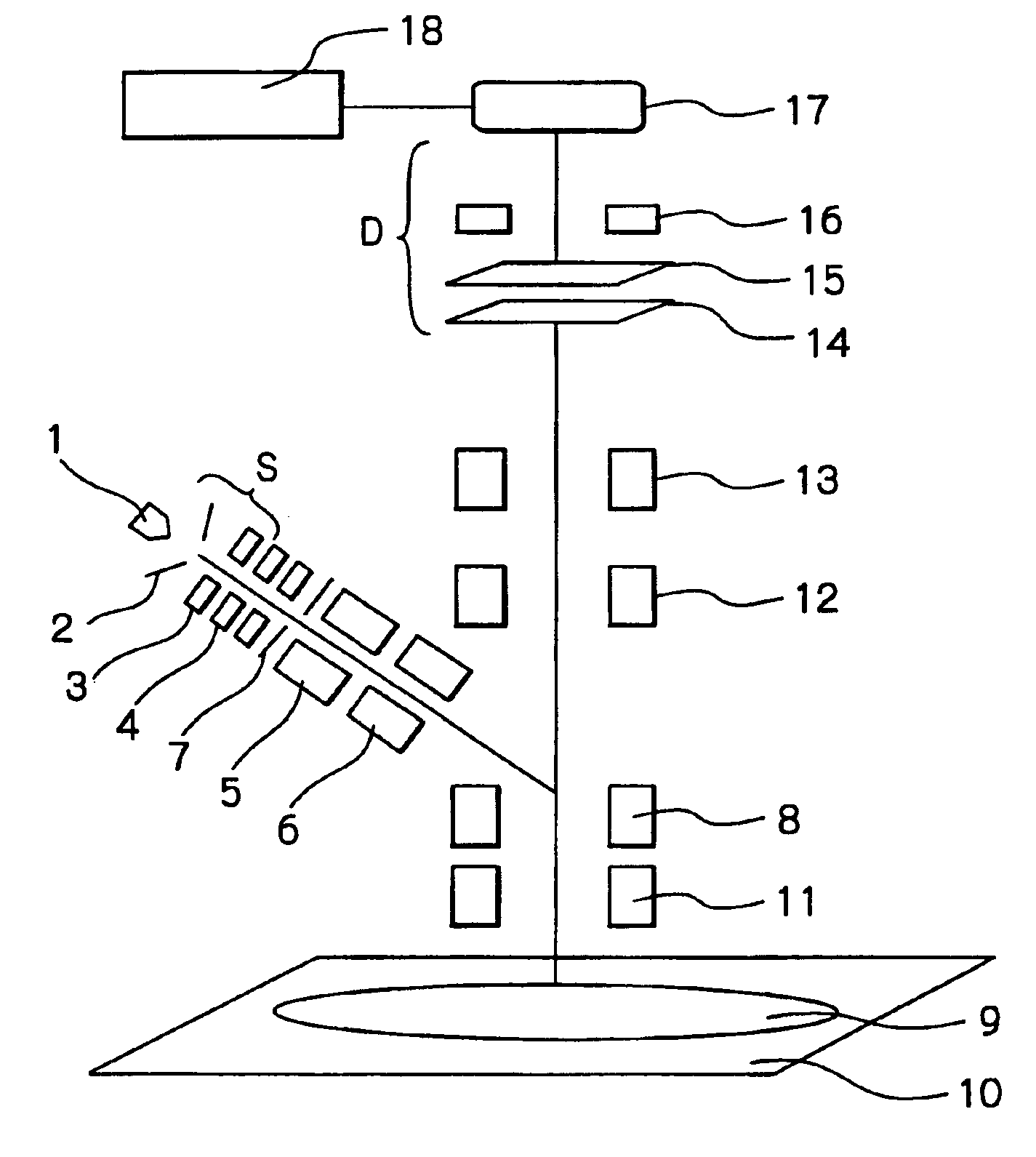
[0028]In the following, several embodiments of an electron beam apparatus according to the present invention will be described in detail with reference to FIGS. 1 to 8. FIG. 1 generally illustrates an electron beam apparatus according to the present invention. The illustrated electron beam apparatus comprises an electron source S which has a cathode 1, a Wehnelt electrode 2 and an anode 3. A primary electron beam emitted from the electron source S is enlarged by three electrostatic lenses, 4, 5, 6, and reshaped by a square aperture plate 7 such that its cross section is formed into a square. The primary electron beam thus reshaped travels in a direction which is bent toward a sample 9 by an ExB filter 8. In this way, the primary electron beam is controlled in terms of an area of the sample 9 irradiated therewith, and irradiation energy, and is irradiated to the sample 9 with a beam of 50 μm×200 μm and irradiation energy of 3 keV. The sample 9 may be a silicon wafer having a diameter...

second embodiment

[0035]The second electron source S′ suitable for use in the second embodiment may comprise a tungsten filament type hot cathode source or a carbon nanotube type cold cathode source, a Wehnelt electrode 2 and an anode 3 in this order. Using nanotube could achieve a process without heat damage by filament heating. With this second electron source S′, the primary electron beam can provide an irradiation region of 10 μm to 10 mm, for example, on the surface of the sample 9 by use of an aperture plate 7 for forming an irradiated area, in which case the irradiation energy can be controlled in a range of 0 to 4 keV, more preferably in a range of 2 to 4 keV.

[0036]FIG. 4 generally illustrates a third embodiment of the electron beam apparatus according to the present invention. As compared with the first embodiment illustrated in FIG. 1, the third embodiment differs in that a laser light source is provided in addition to the electron source S. The following description will be centered only o...

third embodiment

[0038]The laser light source L used herein may be, for example, an He—Cd laser which preferably emits laser light at two wavelengths below 500 nm, specifically at 325 nm and 420 nm, and has an irradiation intensity of 2 W / cm2 or less, more preferably 1 W / cm2 or less, and an irradiating area of 1 mm in diameter. While the third embodiment illustrated in FIG. 4 employs only one laser light source, a plurality of laser light sources may be provided to irradiate the sample 9 with laser light emitted therefrom for increasing the irradiation intensity. Alternatively, the sample 9 may be irradiated with laser light from a plurality of laser light sources in symmetric directions to increase the efficiency.

[0039]FIG. 5 generally illustrates a mapping projection type inspecting apparatus which is a fourth embodiment of the defect detecting apparatus according to the present invention, where components identical or similar to those in the first embodiment illustrated in FIG. 1 are designated b...


PUM

PropertyMeasurementUnit
wavelength bandaaaaaaaaaa
energyaaaaaaaaaa
beam energyaaaaaaaaaa

Abstract

A defect inspecting apparatus is provided for generating a less distorted test image to reliably observe a surface of a sample for detecting defects thereon. The defect detecting apparatus comprises a primary electron beam source for irradiating a sample, electrostatic lenses for focusing secondary electrons emitted from the surface of the sample irradiated with the primary electron beam, a detector for detecting the secondary electrons, and an image processing unit for processing a signal from the detector. Further, a second electron source may be provided for emitting an electron beam irradiated to the sample, wherein the sample may be irradiated with the electron beam from the second electron source before it is irradiated with the primary electron beam from the first electron source for observing the sample. A device manufacturing method is also provided for inspecting devices under processing with high throughput using the defect detecting apparatus.

Description

BACKGROUND OF THE INVENTION[0001]The present invention relates to a defect detecting apparatus which can effectively perform inspections and observations on a surface of a sample such as an evaluation on the structure thereof, an observation in an enlarged view, and an evaluation on materials, an electric conduction state and the like on the surface to detect defects on high density patterns having, for example, a minimum line width of 0.15 μm or less with high accuracy and high reliability, and a device manufacturing method which relies on the defect detecting apparatus to inspect patterns intermediate of a semiconductor device manufacturing process.[0002]In the present invention, the word “mapping” as referred to in the mapping optics means that an electron beam is irradiated on a field of view ranging at least one dimension to form an image of the field of view. Description of the Related Art:[0003]Conventionally, a known testing apparatus detects possible defects on a wafer or a...

Claims


Application Information

Patent Timeline
Patent Type & Authority Patents(United States)
IPC IPC(8): G01N23/225G01N23/22G01N23/00G01K1/08G21K7/00H01J37/244H01J37/285H01J37/29H01J37/04H01J37/05H01J37/26H01L21/66H01J37/22G01Q30/04H01J37/28
CPCH01J37/28H01J2237/2817H01J2237/0044
Inventor NAGAHAMA, ICHIROTAYAMAZAKI, YUICHIROWATANABE, KENJIHATAKEYAMA, MASAHIROSATAKE, TOHRUNOJI, NOBUHARU
Owner EBARA CORP
Why Eureka
Try Eureka