Emission source having carbon nanotube, electron microscope using this emission source, and electron beam drawing device

a carbon nanotube and emission source technology, applied in the manufacture of electric discharge tubes/lamps, instruments, instruments, etc., can solve the problems of inability to observe sufficiently high accuracy, increase the cost, and difficulty in compact device construction, so as to reduce the electrical resistance in the joining portion, increase the amount of electrons supplied to the electron emission site, and prevent the increase of the field emission threshold voltage

Inactive Publication Date: 2005-08-16
HITACHI LTD
View PDF5 Cites 33 Cited by
  • Summary
  • Abstract
  • Description
  • Claims
  • Application Information

AI Technical Summary

Benefits of technology

[0011]Accordingly, an object of the present invention is to provide a high reliability emission source able to sufficiently secure the necessary ohmic contact of the carbon nanotube and an electrically conductive base material, and having sufficient joining strength,and which is a beam shaft adjustment can be made easily.
[0013]In the alternative, the carbon nanotube coming in ohmic contact with the electrically conductive base material is characterized in that this carbon nanotube has an electrically conductive joining material joined to said electrically conductive base material, and a carbon nanotube joined to the electrically conductive joining material. Thus, electric resistance in the joining portion can be reduced, and an increase in the field emission threshold voltage can be prevented, and the amount of electrons supplied to an electron emission site is increased. Further, the amount of heat generated in the joining portion is restrained, and melting, etc. of the electrically conductive base material are prevented, and reliability as the emission source can be increased.

Problems solved by technology

(1) Since no field emission is generated unless a super high vacuum state of 10−8 Pa or more is set, an exhaust system of large-size is required, so that it is difficult to make the device compact, and the cost is increased.
(2) Since no field emission is generated unless the drawing-out voltage is set to high value, such as several kV, an organic material and an organism relating sample, which hold promise for rapid growth in the future, are greatly damaged, and so a sufficiently high accuracy observation can not be made.
However, a new problem exists in that the beam electric current is unstable due to the smallness of the beam electric current and the above-mentioned cause.
Accordingly, the exposure amount of the electron beam, i.e., the exposure time, must be increased to reliably perform the drawing, so that there is the disadvantage of a reduction in efficiency.
However, there is almost no known example in which the single carbon nanotube, or the bundle-shaped carbon nanotube having plural carbon nanotubes apparently set to one bundle, is employed as the emission source of an electron microscope and the electron beam drawing device.
Accordingly, no large electric current can be obtained.
(5) Since the carbon nanotube is attached to the side face of the tungsten needle, it becomes difficult to adjust the electron beam axis after assembly thereof into an electron gun.
However, there is no example of manufacture of the carbon nanotube having excellent electron emission characteristics, while simultaneously satisfying the requirements of crystallinity, purity and fineness of the grown carbon nanotube.
Further, the diameter of the grown carbon nanotube depends on the diameter of the catalyst metallic particle, and it is necessary to arrange one catalyst metallic nano-particle at the electrically conductive needle tip, so that it is very difficult to manufacture.
Therefore, the catalyst metallic particle is lost in the joint of the electrically conductive needle and the carbon nanotube, so that the problems caused by the above-stated joining defect can not be solved.
Further, when the catalyst metallic particle is left, a problem also exists in that plural carbon nanotubes are grown at random from this catalyst metallic particle.

Method used


Image

  • Emission source having carbon nanotube, electron microscope using this emission source, and electron beam drawing device
  • Emission source having carbon nanotube, electron microscope using this emission source, and electron beam drawing device
  • Emission source having carbon nanotube, electron microscope using this emission source, and electron beam drawing device

Examples


embodiment 1

[0026](Embodiment 1)

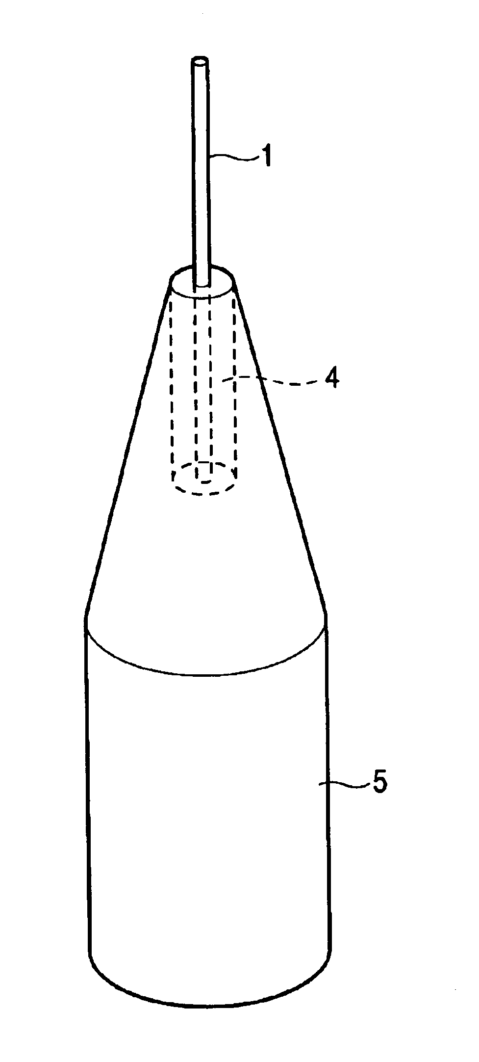
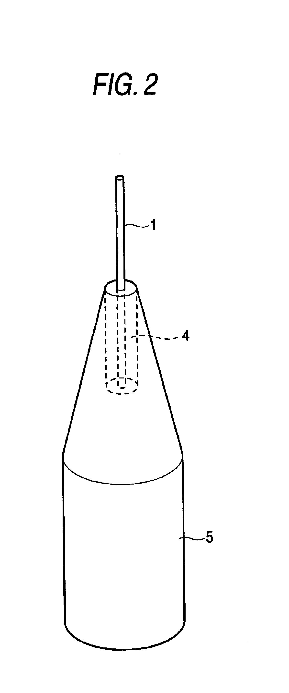
[0027]FIG. 2 shows an emission source in accordance with the present invention. The emission source in accordance with this embodiment has an electrically conductive needle 5 having a micro hole at its tip, an electrically conductive joining material 4 having a melting point lower than that of the electrically conductive needle and arranged in the micro hole, and a carbon nanotube 1 attached to the electrically conductive joining material. Thus, the problem with respect to the joining property of the carbon nanotube and the electrically conductive needle in the emission source can be solved, and the carbon nanotube and the electrically conductive needle can stably come in ohmic contact with each other.

[0028]A metal or carbon excellent electrical conductive property, thermal conductive property and oxidation resisting property, and having a relatively high melting point, is preferable as the material of the electrically conductive needle for attaching the carbon n...

embodiment 2

[0033](Embodiment 2)

[0034]FIG. 4 shows an emission source in accordance with this embodiment The emission source in accordance with this embodiment is constructed such that the carbon nanotube of the emission source described with reference to the embodiment 1 is coated with several layers of an electrically conductive material having a melting point higher than that of the electrically conductive joining material (coating layers are arranged). In accordance with this construction, even when the wettability of the electrically conductive joining material with the carbon nanotube is not so good, the wettability can be improved as a whole and the joining reliability can be raised by nipping a material having good wettability with both the electrically conductive joining material and the carbon nanotube. Further, the ion resisting impact property can be further improved by arranging a coating layer around the carbon nanotube. In this case, when the layer (coating layer) for coating the...

embodiment 3

[0040](Embodiment 3)

[0041]FIG. 5 shows an emission source in accordance with this embodiment.

[0042]The emission source in FIG. 5 is constructed such that this emission source has an electrically conductive plate 5 having a sharp tip shape (tip portion) and a micro hole in its tip portion, an electrically conductive joining material 4 having a melting point lower than that of the electrically conductive needle arranged in the micro hole, and a carbon nanotube 1 attached to the electrically conductive joining material. With respect to the shape of the electrically conductive base material for attaching the carbon nanotube, the tip of the electrically conductive plate is preferably sharp to a certain extent, since an electric field is easily concentrated onto the tip as the tip shape is sharpened.


PUM

PropertyMeasurementUnit
melting pointaaaaaaaaaa
thicknessaaaaaaaaaa
diameteraaaaaaaaaa

Abstract

A high reliability emission source is constructed to secure the ohmic contact between a carbon nanotube and an electrically conductive base material, so as to ensure sufficient joining strength, and to provide for easy beam shaft adjustment. An electron microscope for realizing high resolution, high brightness, a reduction in sample damage due to a reduction in acceleration voltage, a reduction in cost and compactness, and an electron beam drawing device for realizing high definition, high efficiency, a reduction in cost and compactness in comparison with the conventional device, is achieved by using this high reliability emission source. In the emission source, the carbon nanotube is attached to the tip central portion of the electrically conductive base material through an electrically conductive joining material or an organic material by carbonization-processing the organic material by heat treatment, or by diffusive joining.

Description

BACKGROUND OF THE INVENTION[0001]The present invention relates to an emission source having a carbon nanotube, and to an electron microscope and an electron beam drawing device using this emission source.[0002]The following four conditions are required to further increase the resolution and brightness of the electron microscope. (1) The size of the emission source needs to be reduced. (2) The brightness of the emission source needs to be increased. (3) The electron energy width from the emission source needs to be reduced so as to reduce the influence of chromatic aberration. (4) An emitted electron beam needs to be stabilized.[0003]There are various unknown types of electron emission source, including a thermal type made of LaB6, a Schottky type made of ZrO / W, and a field emission type made of tungsten in which the tip of a needle is sharpened by electric field polishing. From the point of view of high resolution and high brightness, the emission source of the field emission type i...

Claims


Application Information

Patent Timeline
Patent Type & Authority Patents(United States)
IPC IPC(8): B82B3/00G03F7/20H01L21/02H01L21/027H01J37/06H01J1/304H01J1/30H01J9/02H01J37/073G01Q70/12H01J37/26
CPCB82Y10/00B82Y30/00H01J1/304H01J37/073Y10S977/876H01J2201/30469H01J2237/0635Y10S977/939C01B32/05H01J9/02H01J37/26
Inventor FUJIEDA, TADASHIHIDAKA, KISHIOHAYASHIBARA, MITSUOSUZUKI, SHUICHINUMATA, YOSHIMICHIHORIUCHI, TOSHIAKI
Owner HITACHI LTD
Why Eureka
Try Eureka