

Processes for hermetically packaging wafer level microscopic structures
a technology of microscopic structure and process, which is applied in the direction of fluid speed measurement, instruments, coatings, etc., can solve the problems of bulky hermetically sealed packaging, adverse effects on the components forming part of the mems device, and high cost of fabrication
Inactive Publication Date: 2005-08-30
RUTGERS THE STATE UNIV
View PDF2 Cites 93 Cited by
- Summary
- Abstract
- Description
- Claims
- Application Information
AI Technical Summary
Benefits of technology
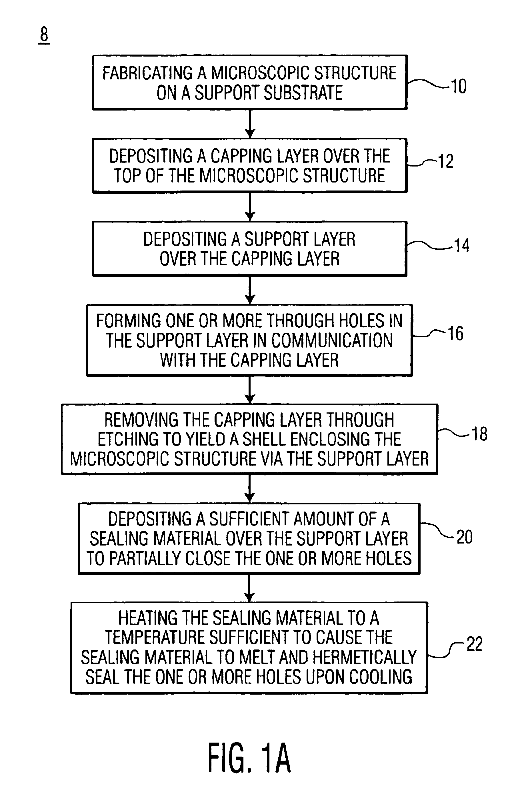
The present invention provides a process for packaging microscopic structures, such as MEMS devices, in a way that creates a cavity containing the device and ensures it remains free of microparticles and undesirable gases that may affect its performance. This process can be used for chip-scale packaging and wafer-level chip-scale packaging, providing a low-cost and highly adaptable approach for batch packaging microscopic structures. The process involves assembling the microscopic structure in a cavity defined by a shell having at least one throughhole, and then applying a molten material to fill the throughhole and create a hermetic pressure seal. This process ensures the microscopic structure remains protected and secure during handling and operation.
Problems solved by technology
Due to their extremely small size, components forming part of the MEMS device can be adversely affected by external factors including RF fields, electromagnetic interference, ambient radiation, dust, gas, shock, sound waves, micro-particles, reactive gases, processing residues, moisture, and the like.
The packaging of MEMS devices are typically not hermetically sealed due to high costs, and are seldom used especially among low cost commercially available packaging.
Such hermetically sealed packaging is typically bulky and expensive to fabricate.
Common structural bonding techniques are generally inadequate to provide good pressure sealing due to surface variations and imperfections.
It is especially difficult to form a high integrity pressure seal if electrical signals must enter or exit the cavity, such as through electrical wires or feedthroughs.
Currently, components of MEMS devices requiring hermetically sealed environments are typically mounted into expensive and relatively large packages formed from multiple components of metal, ceramic or glass material that are welded or soldered together to form a sealed cavity.
To accommodate variations on the surface of the substrate, the package is thicker than the substrate, thus necessitating costly thinning to reduce the thickness.
In addition to requiring precise alignment and thinning, the process typically exposes the MEMS device to high temperature and high voltage conditions that can undesirably damage the MEMS components.
A large amount of contaminants is also undesirably generated from the bonding material used in the packaging process, which can also damage the MEMS device.
However, the time required to precisely align the caps can significantly increase the packaging costs.
Furthermore, the seals formed in the above processes are not generally structurally robust and thus susceptible to leakage and breakage.
Unfortunately, MEMS packaging employing evacuated cavity or pressurized cavities have not been widely adopted in industry because of the high manufacturing costs typically associated with producing MEMS with well-sealed cavities.
These high packaging costs make it difficult to develop commercially viable packaged MEMS devices.
Attempts to implement low cost wafer-level batch processing have typically met with failure due to device design limitations imposed by the lack of an adequate hermetic seal capable of accommodating electrical feedthroughs and wafer level batch processing methods.
As a result, MEMS devices equipped with adequate pressure seal cavities are time-consuming and expensive to produce and have not been widely implemented in industry.
Method used
View moreImage
Smart ImageViewing Examples

Examples
example
Reflow Sealing of Vias Formed in a Silicon Nitride Support Layer
[0073]A thick support layer (1 micron thick) composed of silicon nitride is prepared though sputtering over a microscopic structure. Multiple vias each having a diameter of about 1 micron are etched into the support layer. A copper layer (1 micron thick) is deposited onto the surface of the thick support layer using sputter deposition. An Excimer laser having a wavelength of about 308 nm and a per pulse energy of about 500 mJ focused on a 5 mm by 5 mm spot size is used. The laser is passed through a homogenizer. The laser scans over the copper layer at a rate of about one laser pulse per spot.
Login to View More PUM
| Property | Measurement | Unit |
|---|---|---|
| aspect ratio | aaaaa | aaaaa |
| thick | aaaaa | aaaaa |
| diameter | aaaaa | aaaaa |
Abstract
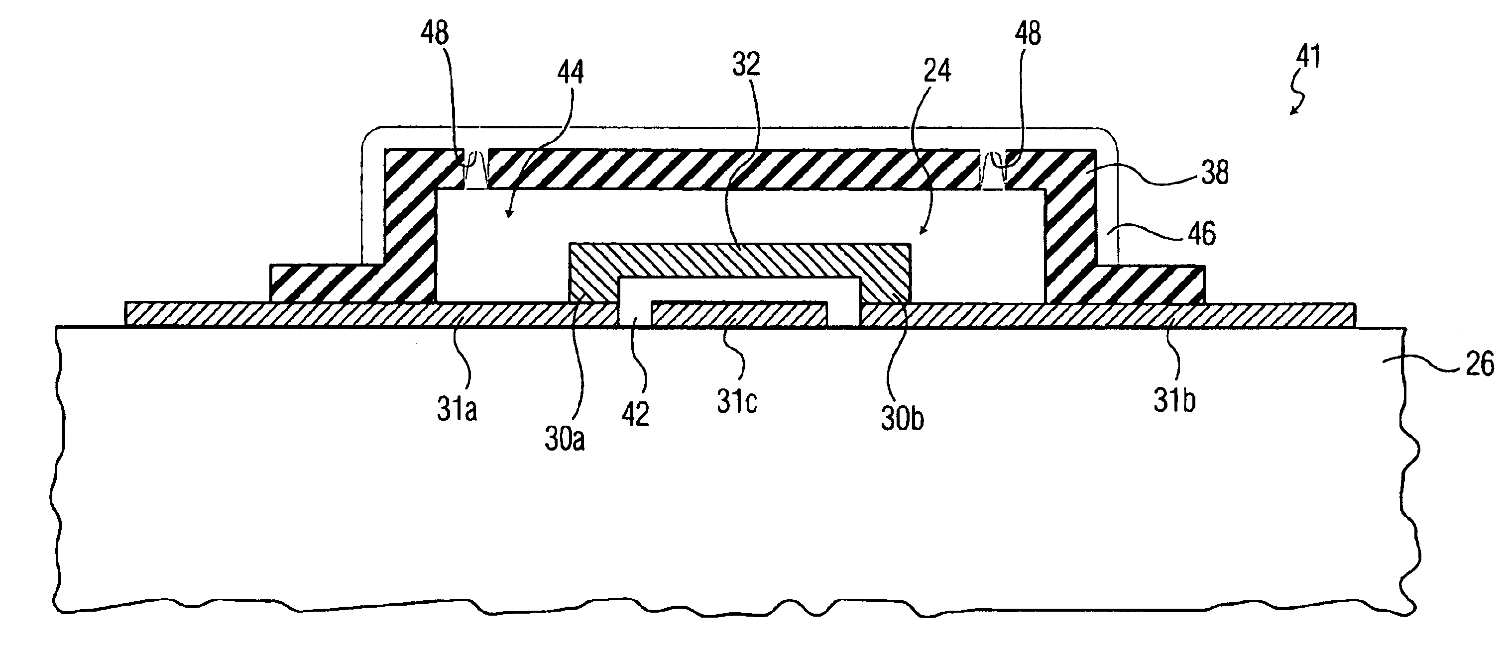
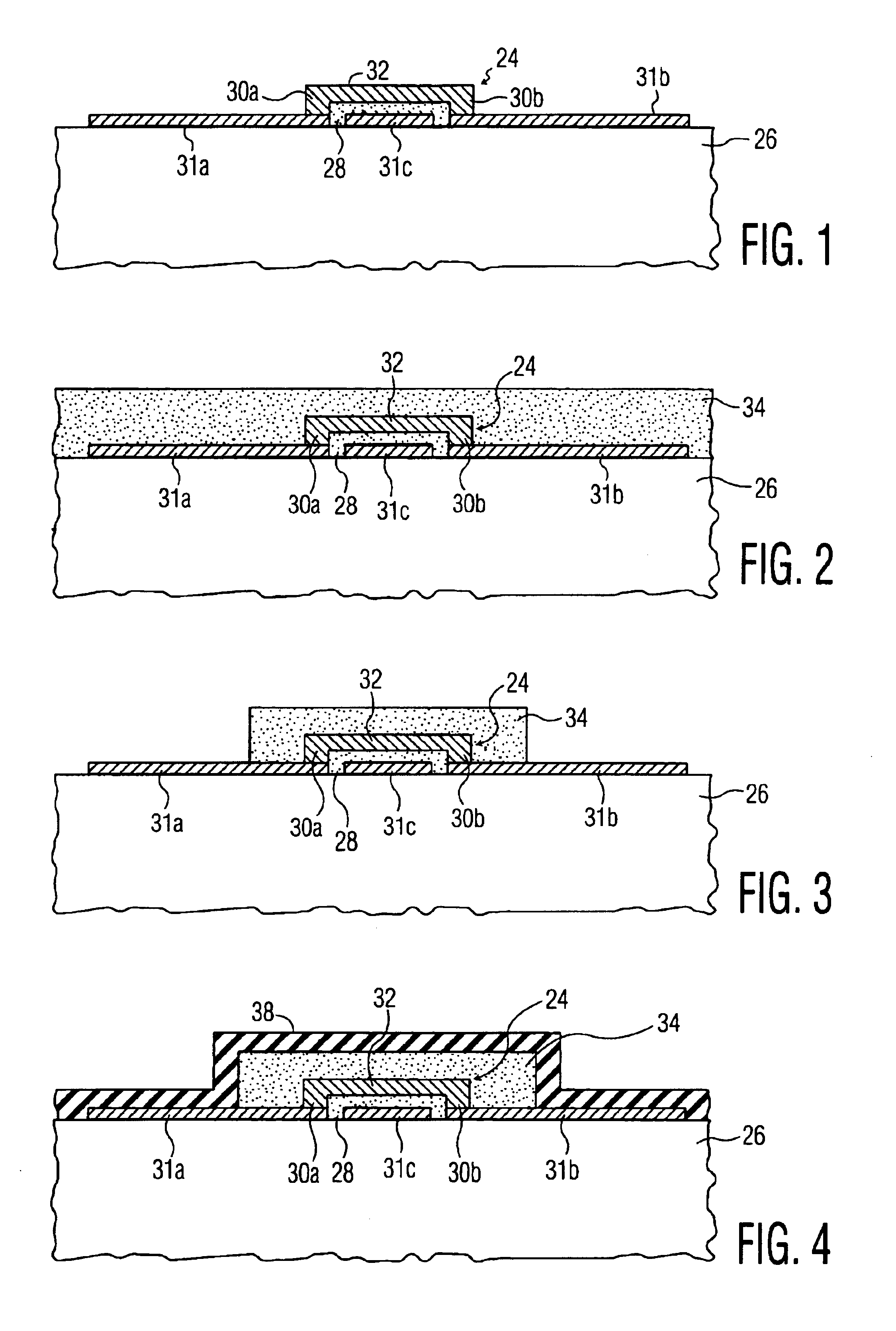
A process for hermetically packaging a microscopic structure including a MEMS device is provided. The process for the present invention includes the steps of depositing a capping layer of sacrificial material patterned by lithography over the microscopic structure supported on a substrate, depositing a support layer of a dielectric material patterned by lithography over the capping layer, providing a plurality of vias through the support layer by lithography, removing the capping layer via wet etching to leave the support layer intact in the form of a shell having a cavity occupied by the microscopic structure, depositing a metal layer over the capping layer that is thick enough to provide a barrier against gas permeation, but thin enough to leave the vias open, and selectively applying under high vacuum a laser beam to the metal proximate each via for a sufficient period of time to melt the metal for sealing the via.
Description
RELATED APPLICATION[0001]This Application claims priority from U.S. Provisional Application No. 60 / 420,322, filed on Oct. 23, 2002, and entitled “METHOD TO PRODUCE LOCALIZED VACUUM SEAL AT WAFER LEVEL FOR LOW COST HIGH RELIABILITY PACKAGING.”FIELD OF THE INVENTION[0002]The present invention is related generally to processes for packaging a microscopic structure, and more particularly to processes for packaging a microscopic structure to produce a microelectromechanical system (MEMS) device having an interior cavity.BACKGROUND OF THE INVENTION[0003]Recent applications of silicon integrated circuit processing technology have led to the development and fabrication of extremely miniaturized devices. Such devices include microelectromechanical systems (MEMS) devices, which consist of an integrated microscopic-scale construction combining electrical and mechanical components. The components of such devices are typically formed and assembled on a silicon substrate using integrated circuit ...
Claims
Login to View More Application Information
Patent Timeline
 Patent Type & AuthorityPatents(United States)
IPC IPC(8): H01L21/70H01L21/00H01L21/8238B81B7/00B81C1/00
CPCB81B7/0077B81C1/00293B81C2203/0145
InventorCHEUNG, KIN P.
OwnerRUTGERS THE STATE UNIV